MV-9_Chapter 5. Teaching.pdf - 第54页
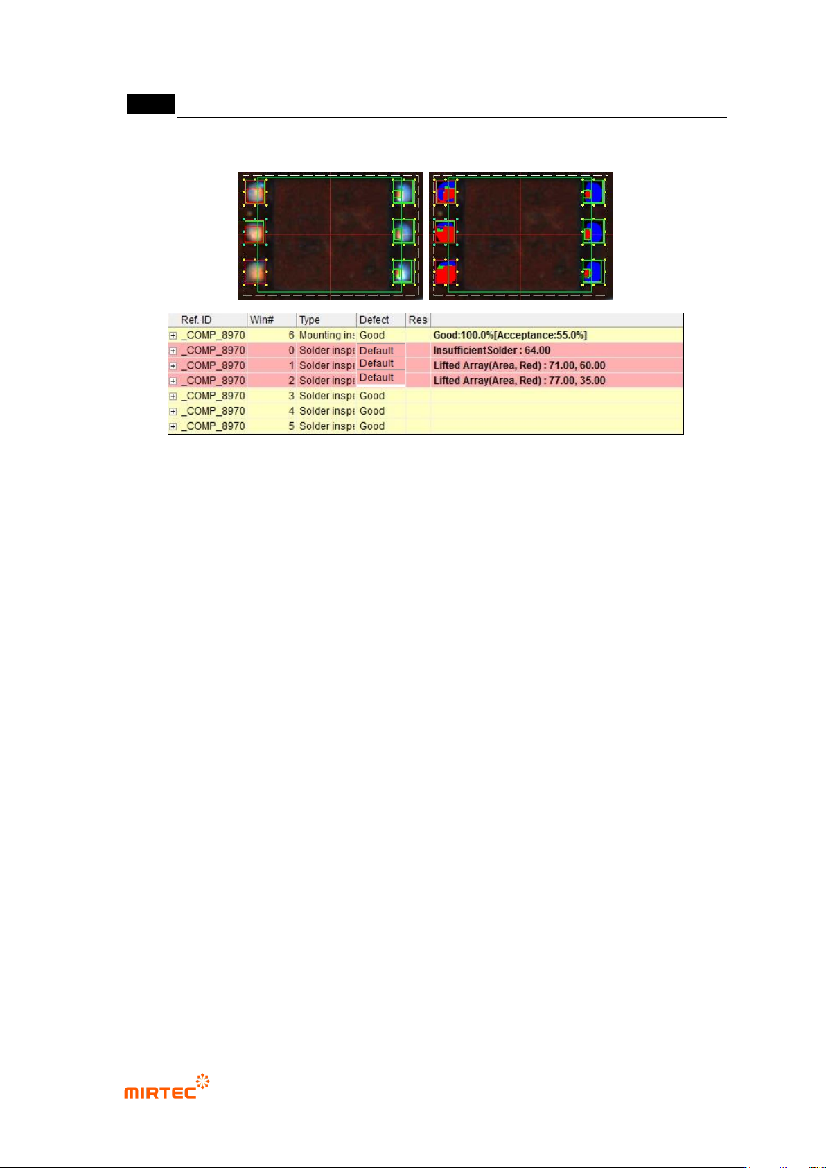
MV -9 Use r Manual 5- 54 [Figure 5- 58 Array inspection result in status screen [Figure 5- 59 Array inspection result example]
错误!使用“开始”选项卡将 제목 2 应用于要在此处显示的文字。错误!使用“开始”选项卡将 제목 2 应用
于要在此处显示的文字。 .
5-53
Stage 2: If stage 1 is normal and total of each RGB area is larger than total red
ratio in preview, judge as good. In this case, center red ratio inspection will not
be conducted.
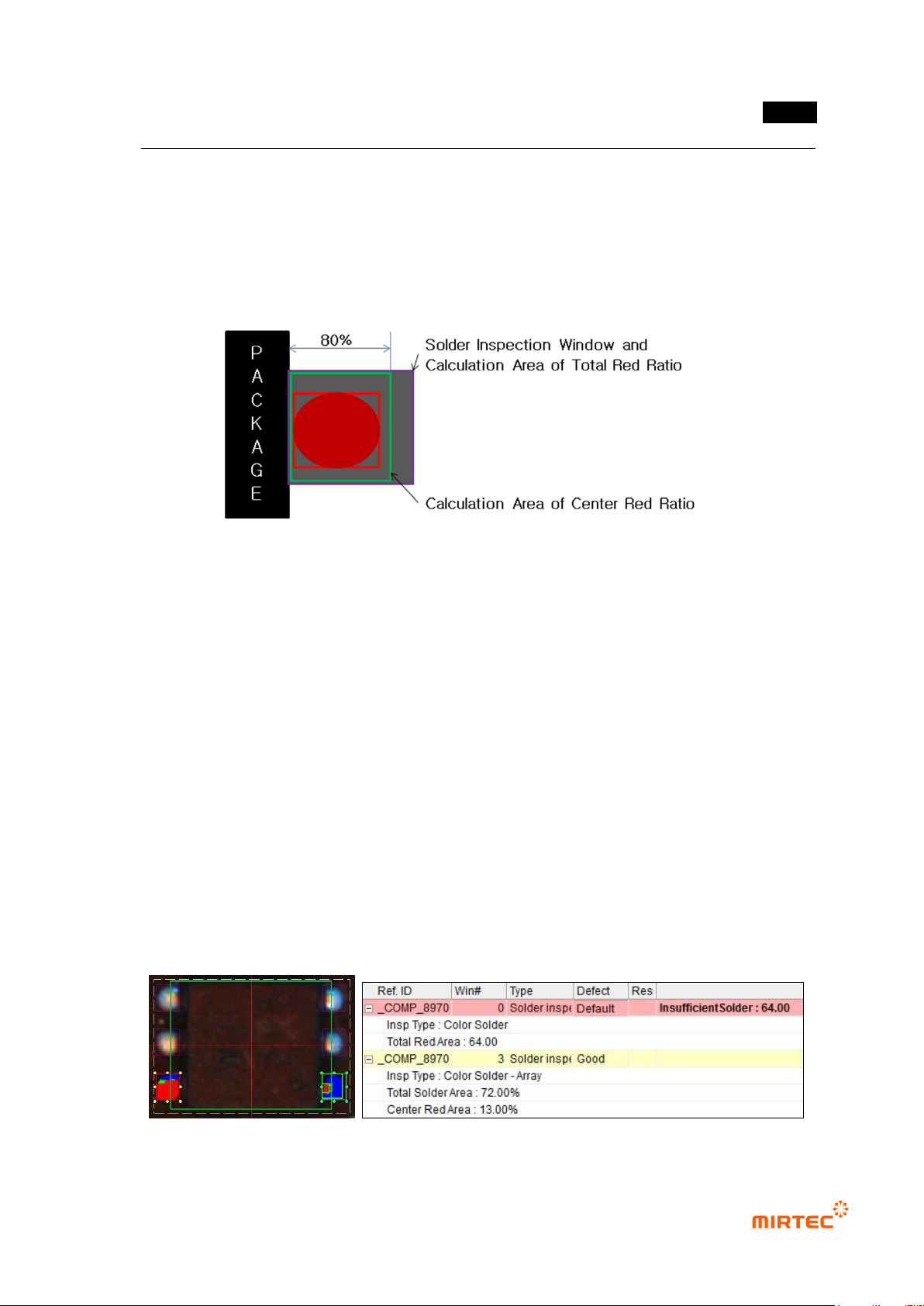
Center red ratio (%): set ratio of red area that exists within 80% range (80% area
from package exterior) of inspection window area. If red ratio is smaller than
reference value, judge as good. If red ratio is larger than reference value, judge as
lifted.
[Figure 5-57 Array solder inspection area]
③ Color inspection – array inspection result in status screen
- Inspection Type: inspection type.
- Total Red Area: ratio of red pixel within whole inspection window area (total red ratio
inspection stage 1).
- Total Solder Area: total pixel ratio of each RGB area within whole inspection window area
(total red ratio inspection stage 2).
- Red Area: ratio of red area in 80% range of inspection window comparing to whole
inspection window area. Inspection result of center red ratio.
- Lifted Array (Area, Red): judged as defect in center red ratio inspection, and area is total
pixel ratio of each RGB area (total red ratio inspection stage 2) result in total inspection
window. Red is calculated value of center red ratio.
- Insufficient Solder: judged as defect in total red ratio inspection. Ratio of red pixel within
whole inspection window area.
MV-9 User Manual
5-54
[Figure 5-58 Array inspection result in status screen
[Figure 5-59 Array inspection result example]
错误!使用“开始”选项卡将 제목 2 应用于要在此处显示的文字。错误!使用“开始”选项卡将 제목 2 应用
于要在此处显示的文字。 .
5-55
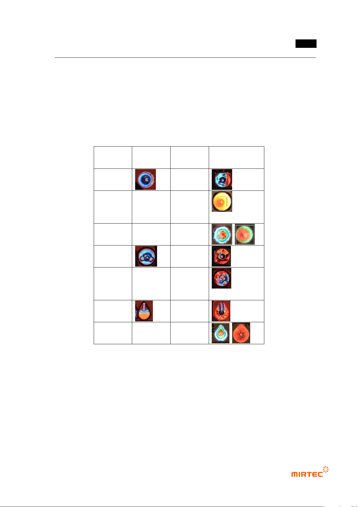
5.3.3.3. Wave Solder inspection
- Algorithm to inspect soldering status for wave soldering that is a soldering process for
manual mounting or auto mounting soldering component. The inspection is divided into pin
type (pin type) and lead type according to component type. In basic defect type, pin is not
exposed, perforation (or defect of hole in solder area due to pin hole, wettability defect).
[Table 5-4 4 Binarization methods of solder amount inspection window]
Type
Normal
image
Defect
name
Defect image
pin type
perforation
No solder,
insufficient
solder
no pin
exposure
perforation
No solder,
insufficient
solder
lead type
perforation
no pin
exposure
1) Teaching method
① Click <soldering inspection window> button among operating buttons.
② Draw inspection window in solder area.
③ Select horizontal + vertical light for light type. Image type will be automatically selected.
④ Adjust position and size of pin inspection area and solder inspection area.
⑤ Adjust color map and binarization value checking preview.
⑥ Enter inspection criteria.