MV-9_Chapter 5. Teaching.pdf - 第34页
MV -9 Use r Manual 5- 34 [Figure 5- 36 mounting inspection windo w inspection result scr een] S hape - This is to displa y inspe ct i on type (inspect i on a lg o rithm). Defect name - This is to display inspection r…
错误!使用“开始”选项卡将 제목 2 应用于要在此处显示的文字。错误!使用“开始”选项卡将 제목 2 应用
于要在此处显示的文字。 .
5-33
Use max matching ratio
- This is to conduct pattern matching of all registered pattern images. Compare the highest
matching ratio with reference value to judge good/defect.
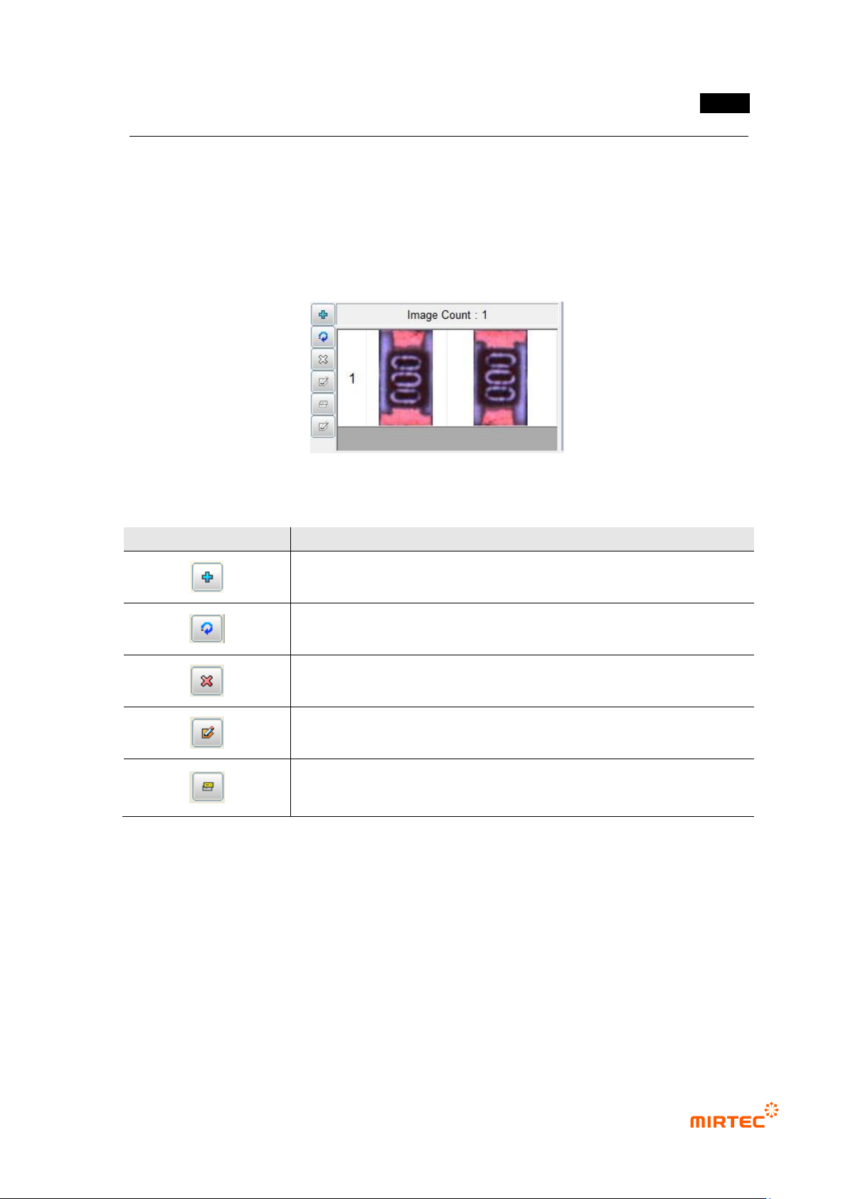
Pattern image screen
- This screen is to display pattern image registered during mounting inspection and chip
inspection.
[Figure 5-35 Pattern image screen]
[Table 5-2 Description of operating buttons]
icon
Name and Description
Current image add: add current image.
Current image refresh: re-image current image.
Current image delete: delete current image.
Mask image edit („Don‟t care region‟ setting): set unnecessary image
region to skip it during inspection.
Image synchronization: select specific pattern image and click
synchronization button to set „Don‟t care region‟ of a specific pattern at
once.
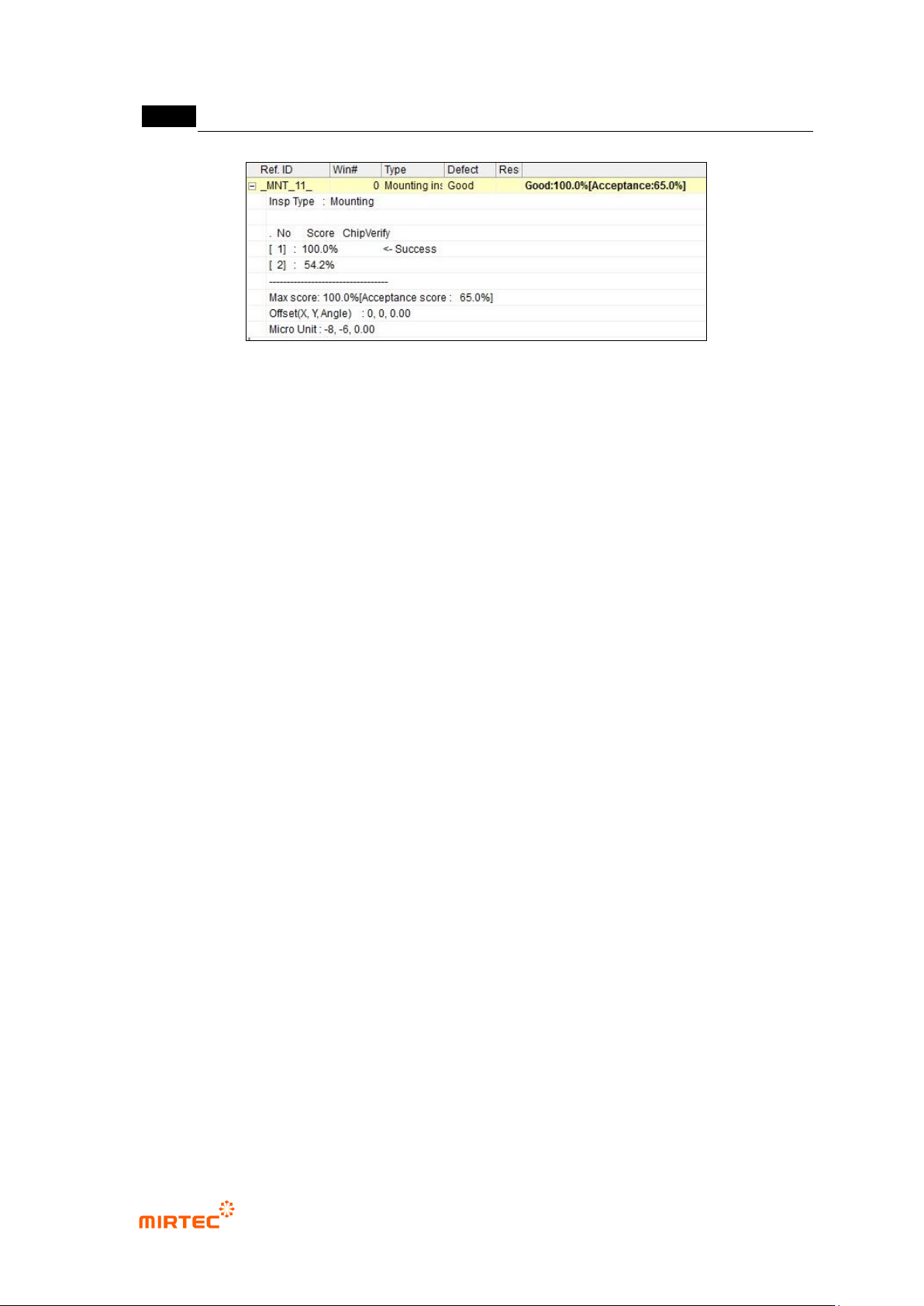
4) Inspection result in status screen
- To directly inspect mounting inspection window that completed teaching, select inspection
window and select „Inspect‟ in popup menu displayed by clicking right button of the mouse
or press enter key to start inspection. The following inspection result will be displayed in
inspection result screen on the bottom of the main screen after inspection.
MV-9 User Manual
5-34
[Figure 5-36 mounting inspection window inspection result screen]
Shape
- This is to display inspection type (inspection algorithm).
Defect name
- This is to display inspection result and item selected at good/defect type.
No
- Number in square bracket means the order of registered pattern image for the relevant
component. If polarity is not set among inspection options, images rotated for one sub
image will be inspected at the same time. Hence, there will be 2 models.
Matching ratio
- The value displayed in percent is matching ratio between image registered in pattern
image screen and imaged image.
Chip re-inspection
- Chip re-inspection result will be judged and displayed by „O/X‟.
Success
- This will be displayed for a model that successfully completed matching among registered
many models.
Max matching ratio
- This is to display max matching ratio among the registered models. Percent in brace
means normal judgment matching score.
Offset (x, y)
- This is to display offset value from the center of inspection window to the center of
component found in search area in pixel unit.
错误!使用“开始”选项卡将 제목 2 应用于要在此处显示的文字。错误!使用“开始”选项卡将 제목 2 应用
于要在此处显示的文字。 .
5-35
5.3.3. Solder inspection window
- Solder inspection is divided into general inspection, color inspection, and wave solder
inspection, and inspection for solder part of mounted component will be conducted.
General inspection: This is used to inspect no solder, insufficient solder and excessive solder
and defects of solder part of component. Besides basic soldering inspection, general
inspection can selectively conduct non-mounting inspection (soldering) and non-mounting
inspection (mounting).
Color inspection: surface crack defect inspection of BGA or CSP (chip scale package) or
soldering status inspection of array component can be selectively conducted.
Wave solder inspection: This is to inspect soldering status of manual mounting component by
flow or wave soldering process.
5.3.3.1. General inspection
1) Soldering inspection (basic)
① Teaching method
- Click <soldering inspection window> button among operating buttons.
- Draw inspection window in soldering area desired to be inspected.
- Select light type of horizontal + vertical light ( ) in which soldering area of component is
clear and select B (blue) for image type.
- Select preview, and adjust binarization method and binarization value for good separation
of soldering area. If soldering area does not separated well, check color map and select
setting to set color and saturation range.
- Enter normal criteria.