MV-9_Chapter 5. Teaching.pdf - 第36页
MV -9 Use r Manual 5- 36 [Figure 5- 37 Screen to cr eate soldering inspection (basic) window] ② Parameter of soldering inspection (basic) window Reference name - Refer to „ reference name (page5- 21 ) ' i n „5.3.1…
错误!使用“开始”选项卡将 제목 2 应用于要在此处显示的文字。错误!使用“开始”选项卡将 제목 2 应用
于要在此处显示的文字。 .
5-35
5.3.3. Solder inspection window
- Solder inspection is divided into general inspection, color inspection, and wave solder
inspection, and inspection for solder part of mounted component will be conducted.
General inspection: This is used to inspect no solder, insufficient solder and excessive solder
and defects of solder part of component. Besides basic soldering inspection, general
inspection can selectively conduct non-mounting inspection (soldering) and non-mounting
inspection (mounting).
Color inspection: surface crack defect inspection of BGA or CSP (chip scale package) or
soldering status inspection of array component can be selectively conducted.
Wave solder inspection: This is to inspect soldering status of manual mounting component by
flow or wave soldering process.
5.3.3.1. General inspection
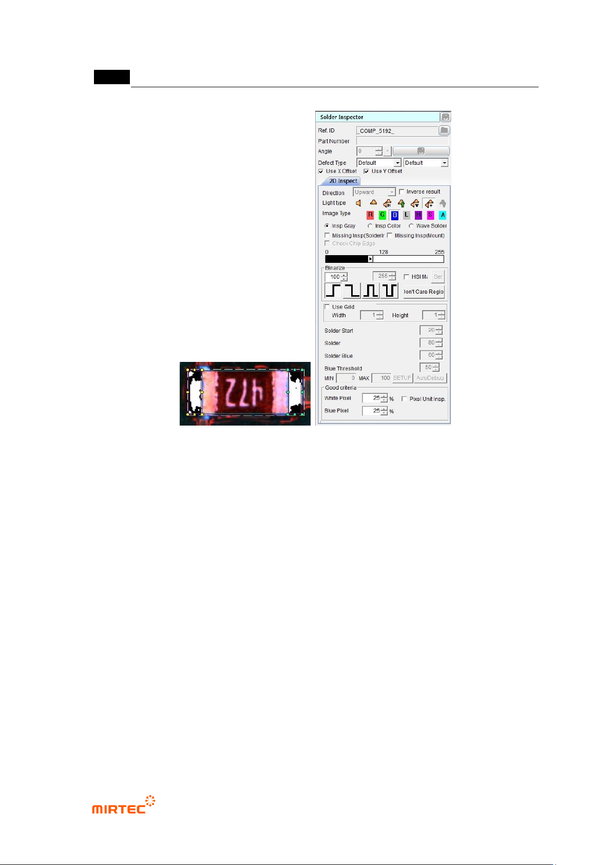
1) Soldering inspection (basic)
① Teaching method
- Click <soldering inspection window> button among operating buttons.
- Draw inspection window in soldering area desired to be inspected.
- Select light type of horizontal + vertical light ( ) in which soldering area of component is
clear and select B (blue) for image type.
- Select preview, and adjust binarization method and binarization value for good separation
of soldering area. If soldering area does not separated well, check color map and select
setting to set color and saturation range.
- Enter normal criteria.
MV-9 User Manual
5-36
[Figure 5-37 Screen to create soldering inspection (basic) window]
② Parameter of soldering inspection (basic) window
Reference name
- Refer to „reference name (page5-21) ' in „5.3.1 mounting inspection window‟‟ excepting
shape.
- Created in „_SLD_1_‟ format. „SLD‟ means Solder and number means creation order of
solder amount inspection window.
Component name
- Refer to „component name‟ in '5.3.1 mounting inspection window‟‟.
Rotation angle
- Refer to „rotation angle‟ in '5.3.1 mounting inspection window‟‟.
Defect type
- Refer to „defect type‟ in '5.3.1 mounting inspection window‟.
Light type
- Select light type and image type in which soldering area of component is clear.
错误!使用“开始”选项卡将 제목 2 应用于要在此处显示的文字。错误!使用“开始”选项卡将 제목 2 应用
于要在此处显示的文字。 .
5-37
- Since soldering area is slope on PCB, light type of horizontal + vertical light ( ) and
image type of B (blue) for slope area are recommended. L (luminance) can be also
selected.
- If necessary, select horizontal - vertical ( ) or L (luminance). Vertical white light and
horizontal white light are used to create horizontal - vertical image.
Image type
- In case of horizontal + vertical light, select B or L for image type. In case of horizontal -
vertical, select L for image type.
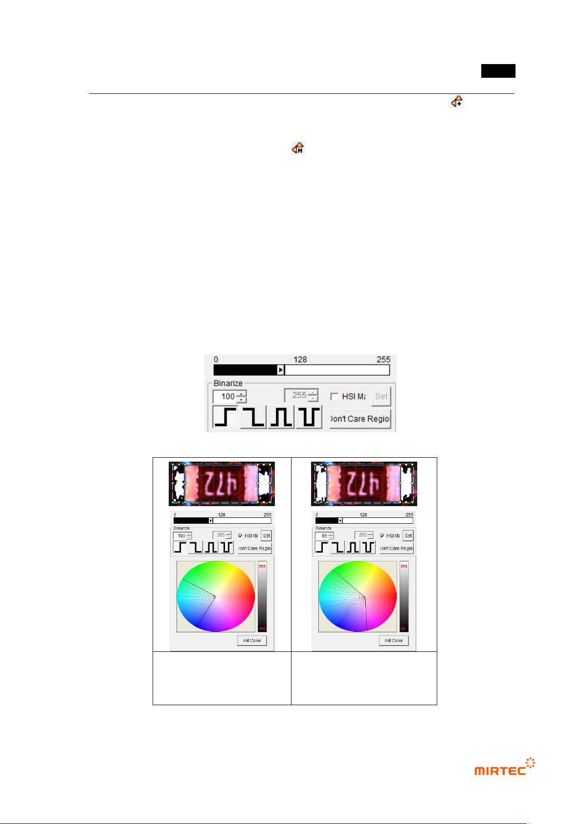
Binarization
- This means to express images in white (1) and black (0) for black and white image that is
express by 256 steps based on specific level value(binarization value).
- User can adjust desired color, saturation and luminance area for image type selected
using color map.
- To check binarized image in frame image screen, click <preview> button in „operating
buttons‟. [Table5-3] shows 4 binarization methods.
[Figure 5-38 Binarization value setting]
Binarization image in initial
status of color map
Binarization image after
adjusting color map and
binarization
[Figure 5-39 Binarization value setting]