MV-9_Chapter 5. Teaching.pdf - 第108页
MV -9 Use r Manual 5- 108 2) T eaching outline - Draw window and conduct 4 steps of sett i ng for IC/Bridge inspection . Draw w i ndow to set default param eter accor ding to the image in the current screen. However , pa…
错误!使用“开始”选项卡将 제목 2 应用于要在此处显示的文字。错误!使用“开始”选项卡将 제목 2 应用
于要在此处显示的文字。 .
5-107
[Figure 5-113 IC lead Bridge inspection area]
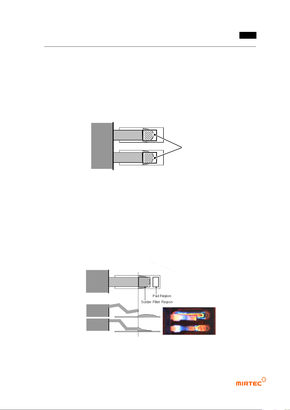
Solder defect
- If reflow is skipped, lead on pad is melt and shows burning shape after IC component is
mounted by mounter. There should be enough amount of lead to fix it on the pad. However,
if screen printer incompletely applies lead, small amount of lead is applied to some pad
area, and there will be problem of fixing of IC component after reflow. This solder defect is
called as no solder or insufficient solder. Therefore, lead amount in solder fillet area must
be inspected to detect solder defect.
- This system uses image that binarized inspection area to judge solder defect.
[Figure 5-114 IC lead solder inspection area]
Lifted defect
- If lead of mounted IC component is vertically bent or one side of component itself is slope
and lifted from substrate during mounting, lead is not soldered on pad. This is called lifted
defect.
- To inspect defect of IC lead, inspect position of lead tip and lead color in lead area, and
inspect solder paste status in solder fillet area and pad area.
- This system judges lifted defect of IC lead using color information and luminance
information in each inspection area.
[Figure 5-115 IC lead lifted inspection area]
Inspection area
역
MV-9 User Manual
5-108
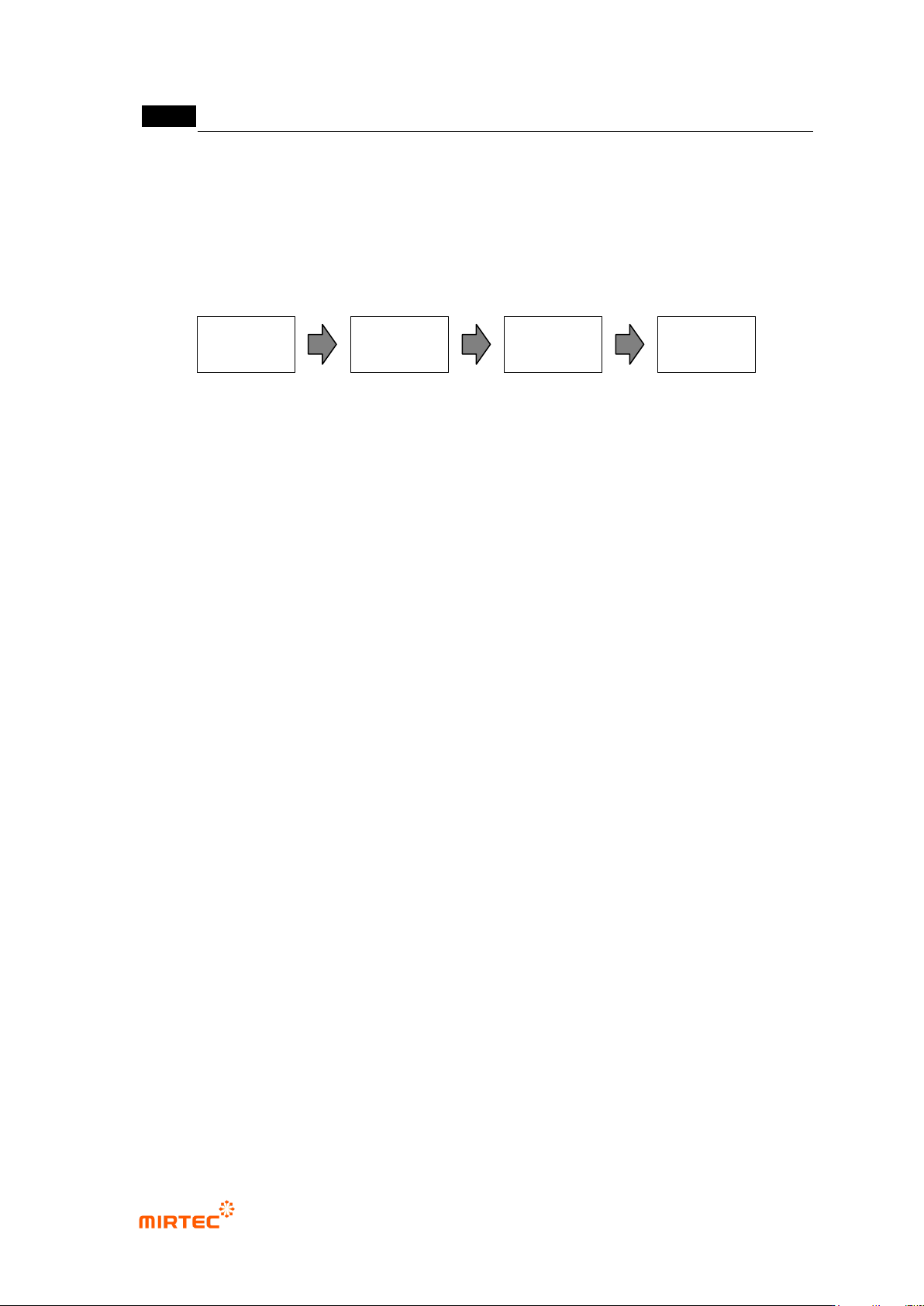
2) Teaching outline
- Draw window and conduct 4 steps of setting for IC/Bridge inspection. Draw window to set
default parameter according to the image in the current screen. However, parameter
setting according to the following steps is recommended to increase inspection
performance.
[Figure 5-116 IC/Bridge inspection setting steps]
Bridge inspection area setting: lead separation tap
- Basically, this is to get gap area that is inspection area for bridge inspection. set light and
parameter for good lead separation of window area.
- In general, select R (red) for image type in horizontal + vertical light, and use an image that
applied high binarization value and noise removal.
Bridge inspection: Bridge inspection tap
- set light and parameter in which bridge can be defected well in gap area from lead
separation.
- In general, select B (blue) for image type in horizontal + vertical light, and use image with
low binarization value and no noise removal.
- In case of PCB with much amount of flux, remove flux by performing some noise removal.
Solder inspection area setting: lead tip tap
- Set parameter of lead tip tap to set area to detect solder defect. the most important
parameter on lead tip tap is to set to automatically achieve or user manually achieve using
the characteristic of which profile of end part appears low when profile is achieved through
lead image at position of lead end.
- In general, use image that completed auto binarization and some noise removal in vertical
light to detect automatically lead tip.
- Intersection area between lead tip position and lead area from lead separation will be
solder inspection area.
Solder inspection: solder amount inspection tap
- Conduct solder inspection for solder fillet area set in solder inspection area setting. Set
parameter for light and good/defect judgment suitable for solder inspection.
- In general, select B for image type in horizontal + vertical light. Sometimes horizontal –
vertical is selected. At this point, image type is automatically set to „L‟.
- Select use of lifted inspection and set parameter for good/defect judgment.
Bridge
inspection area
setting
Bridge
inspection
Solder
inspection area
setting
Solder
inspection
错误!使用“开始”选项卡将 제목 2 应用于要在此处显示的文字。错误!使用“开始”选项卡将 제목 2 应用
于要在此处显示的文字。 .
5-109
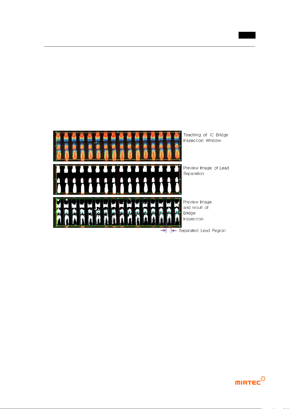
3) IC Bridge inspection teaching method
- Conduct inspection of short between lead and lead for IC Bridge inspection.
① Click <IC/Bridge inspection window> button among operating buttons.
② Draw inspection window in IC lead area to be inspected.
③ Select lead separation tap. Select light type and image type for good lead separation
checking preview. In case of noise around lead, use noise removal function. Check for good
lead separation through trial inspection.
④ Select Bridge inspection tap, and select proper light type and image type to detect foreign
material between lead checking preview.
[Figure 5-117 IC Bridge teaching]
4) Solder amount inspection (general inspection) teaching method
- For solder amount inspection (general inspection), extract using binarization method that
used luminance information of inspection image or designation of color area for inspection
using color map adjustment, and conduct inspection by applying binarization method.
① Create inspection window using IC Bridge inspection teaching method.
② In case of conducting solder amount inspection, check at solder amount inspection over lead
separation tap.
③ Set lead tap position and solder inspection area on lead tip tap. Lead tip position can be
manually or automatically set.
④ Select solder amount inspection tap, select white tap of central part and enter normal criteria
to judge good/defect. In case of conducting lifted inspection, check lifted inspection, and
enter good/defect judgment criteria.