N7201A616E00_0317.pdf - 第365页
NPM-W 2 EJM7DE-MB-06O-0 0 Lamp value of lamps 1 to 4. 6-1-3 -2 B A C D Lighting Size Choose a recognition mark color. E Choose a light adjustmen t method. F Changes to the previous or next screen. Shape selection Search …
NPM-W2 EJM7DE-MB-06O-00
Data
editing
6-1-3-1
D
A
B
E
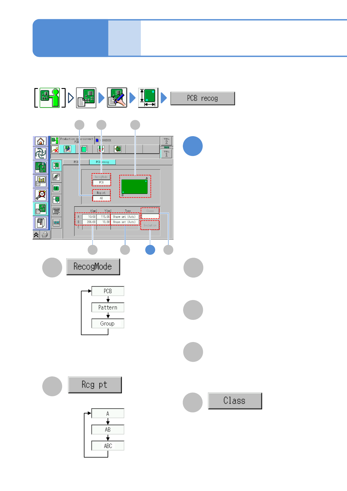
Choose a recognition mark.
D E
AB
If [Pattern] or [Group] is selected in the
recognition mode and there are several
types, choose the pattern number or
group number.
F
1
Edit the data of the desired
field on the screen
Choose a recognition mode.
●PCB: Recognizes the PCB recognition mark
●Pattern: Recognizes the pattern recognition
mark
●Group: Recognizes the group recognition mark
PCB recognition data
edit 1
Describes how to edit the PCB recognition data registered by DGS.
Enter the PCB recognition coordinates
(X,Y) of each recognition mark.
●Touching the screen opens the input
window.
F
Type
The recognition method for each
recognition mark. Pressing the [Type]
field causes the shape setting screen of
each recognition mark to appear .
C
C
Illustration of a recognition mark (A or B or
ABC).
Recognition position on a PCB
3
Operating procedure
6-1-3
X[mm], Y[mm]
NPM-W2 EJM7DE-MB-06O-00
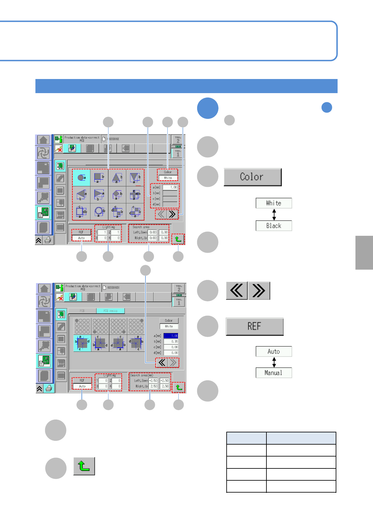
Lamp value of lamps 1 to 4.
6-1-3-2
B
A
C
D
Lighting
Size
Choose a recognition mark color.
E
Choose a light adjustment method.
F
Changes to the previous or next screen.
Shape selection
Search area
H
G
E F G
DA C B
Returns to the previous screen.
Shape selection and edit
Size of a selected recognition mark
shape.
●Touching the screen opens the input
window.
Recognition range of one recognition mark.
●Touching the screen opens the input window.
Choose a recognition mark shape.
H
E F G
D
H
2
By the step of (P.6-1-3-1)
1
E
(type)
●Relationship between a head camera
lighting and lighting (P.7-3-16)
Lighting Type
1 Coaxial lighting
2 High angle lighting
3 Middle angle lighting
4 Low angle lighting
Setting
change
NPM-W2 EJM7DE-MB-06O-00
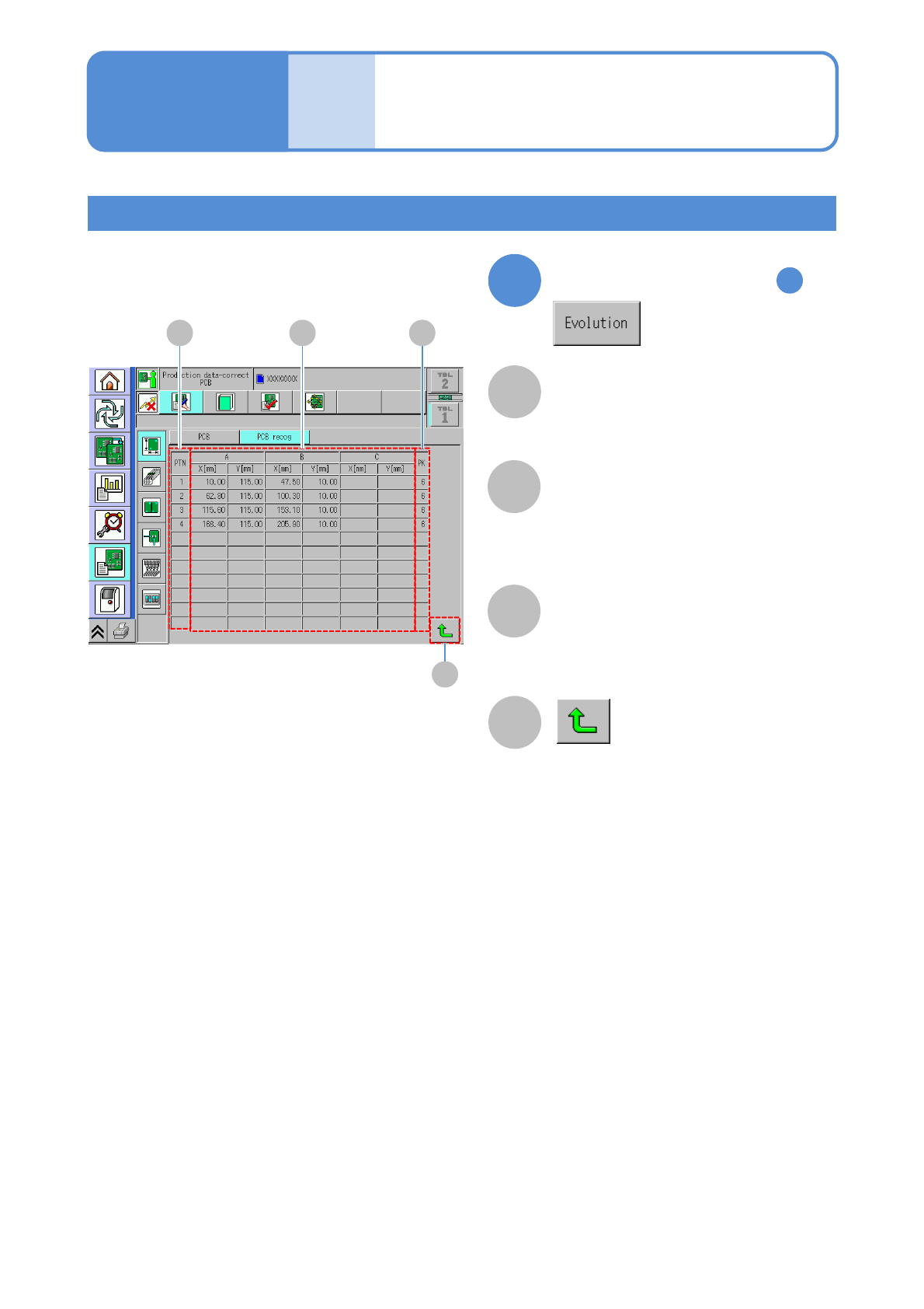
C
B
PCB recognition coordinate of a
recognition point (X,Y)
Number to arrange several types of patterns.
A
Pattern number.
6-1-3-3
Data
editing
PCB recognition data
edit 2
Expanded data display
3
PK
PTN (pattern)
D
Returns to the previous screen.
Operating procedure
6-1-3
By the step of (P.6-1-3-1)
1
A B C
D
X[mm], Y[mm]