N7201A616E00_0317.pdf - 第680页
NPM-W 2 EJM7DE-MB-09O -00 A pplica ble PCB specifica tions 2 9-1-4 -3 Item Common PCB cutout condition PCB cutout size sho uld meet the following two condition s. ■ Condition A PCB cutout size should meet the following c…
NPM-W2 EJM7DE-MB-09O-00
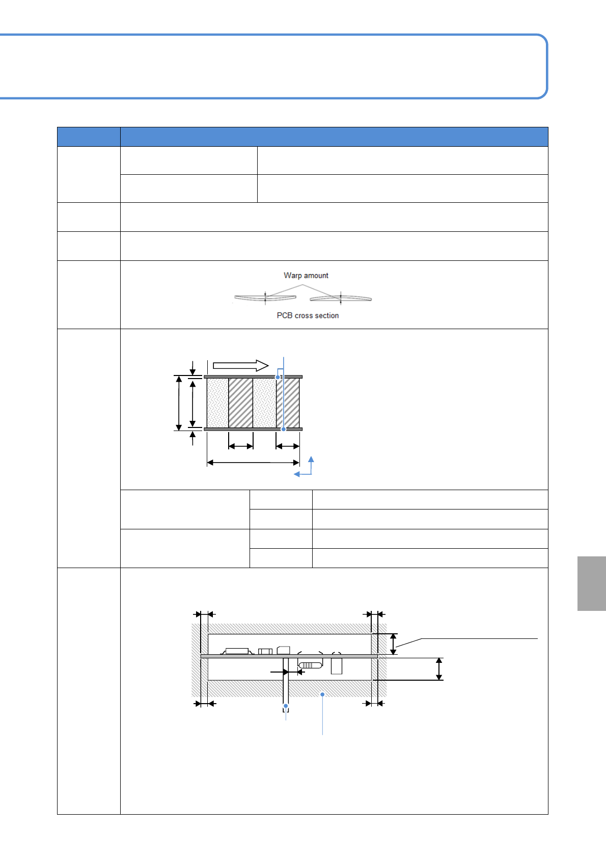
Item Dual conveyor
Dimensions
(mm)
Dual lane mode
●Min. : L 50 W 50 ●Max.: L 750 W 260
Single lane mode
●Min.: L 50 W 50 ●Max.: L 750 W 510
Thickness
(mm)
0.3 to 8.0 (Dot dispensing: 0.5 to 8.0 )
Mass (kg)
3 or under (after placement)
Allowable
PCB warp
(mm)
Placement
and
dispensing
area
(mm)
Single lane mode Placement a: 50 to 510 b: 44 to 504 c: 3.0 d: 50 to 750
Dispensing a: 50 to 510 b: 42 to 502 c: 4.0 d: 50 to 750
Dual lane mode Placement a: 50 to 260 b: 44 to 254 c: 3.0 d: 50 to 750
Dispensing a: 50 to 260 b: 42 to 252 c: 4.0 d: 50 to 750
Dead
space
(mm)
9-1-4-2
3
28
No component area
PCB support pin
Keep 2 mm away from the component on the reverse side.
●If you want to create your own PCB-support blocks, please consult us.
Warp lower: within 0.5
Warp upper: within :0.5
3
3
3
*1)
*1)
16-nozzle head : Max. 6.5
12-nozzle head : Max. 6.5
8-nozzle head : Max. 12
3-nozzle head : Max. 30
Dispensing head : Max. 28
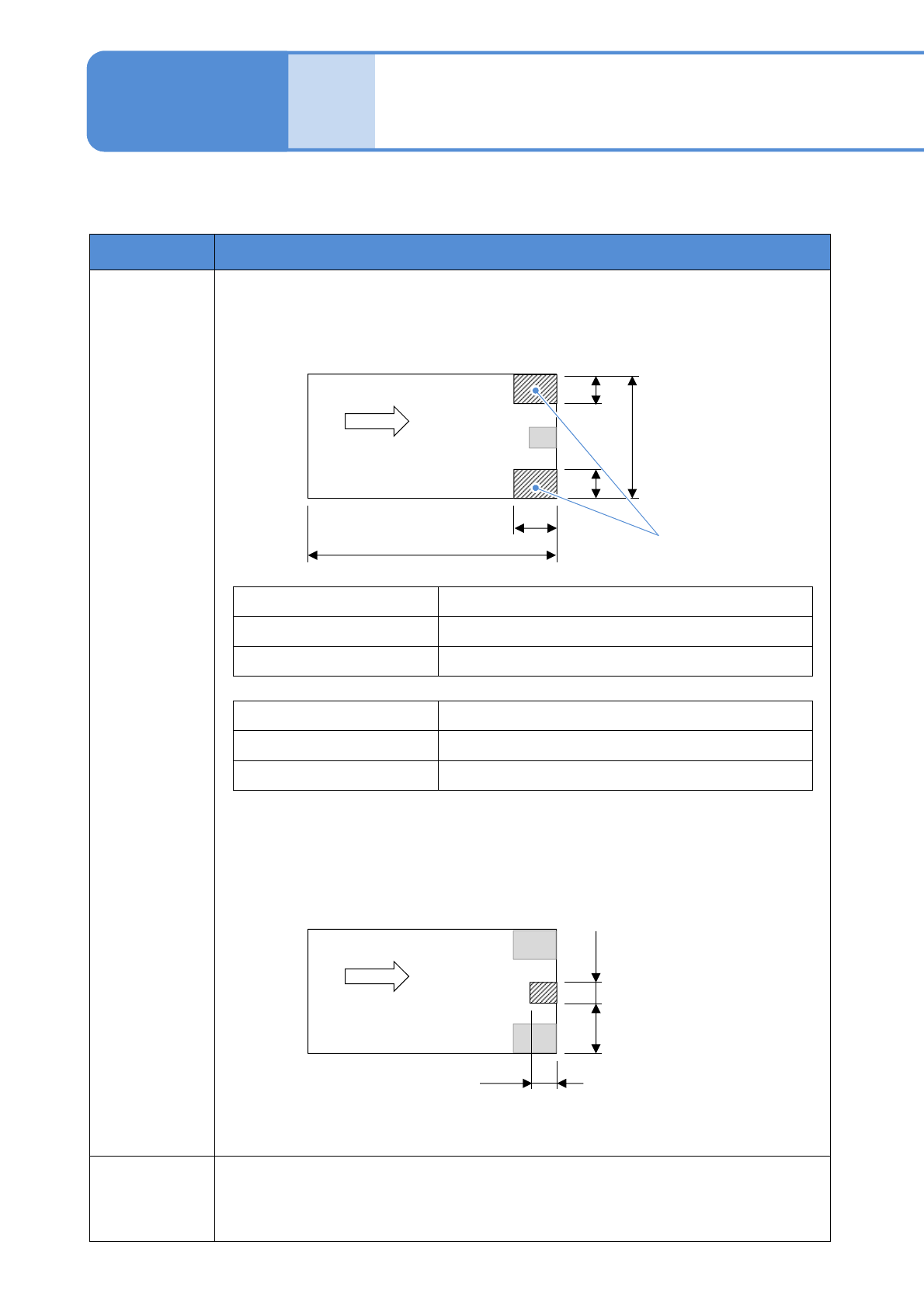
At
a glance
No component
area
Y
X Fixed side
Placement area
a: 50 to 550
b: 44 to 542
c: 3.0
d: 50 to 750
d
1,d2: 50 to 350
*1)
Dispence area
a: 50 to 550
b: 42 to 542
c: 4.0
d: 50 to 750
d
1,d2: 50 to 350
*1)
a b
c
d
c
d2 d1
PCB flow
*1) When two PCBs are clamped
NPM-W2 EJM7DE-MB-09O-00
Applicable PCB
specifications 2
9-1-4-3
Item Common
PCB cutout
condition
PCB cutout size should meet the following two conditions.
■Condition A
PCB cutout size should meet the following condition.
■Condition B
There should be no cutout (including slit) in the area B shown below.
PCB
projection size
from PCB
edge
Consult us.
L
L1
50 mm ≦ L ≦ 350 mm
L/4 or less
350 mm < L ≦ 750 mm
Smaller one of either L/4 or 100 mm
●Above described condition is when the PCB thickness is less than1.6 mm. If the
PCB thickness exceeds 1.6 mm, please consult us.
W
W1
50 mm ≦ L ≦ 260 mm
Smaller one of either W/3 or 30 mm
260 mm < L ≦ 550 mm
Consult us separately
Transport
direction
L
L1
A
A
W1
W1
W
Any of one location
30mm
Transport
direction
10mm
B
10mm
●If there is cutout (including slit) in the above area, please consult us.
Specifi-
cation
Operating procedure
9-1-4
NPM-W2 EJM7DE-MB-09O-00
9-1-4-4
At
a glance
Item Common
PCB
recognition
mark
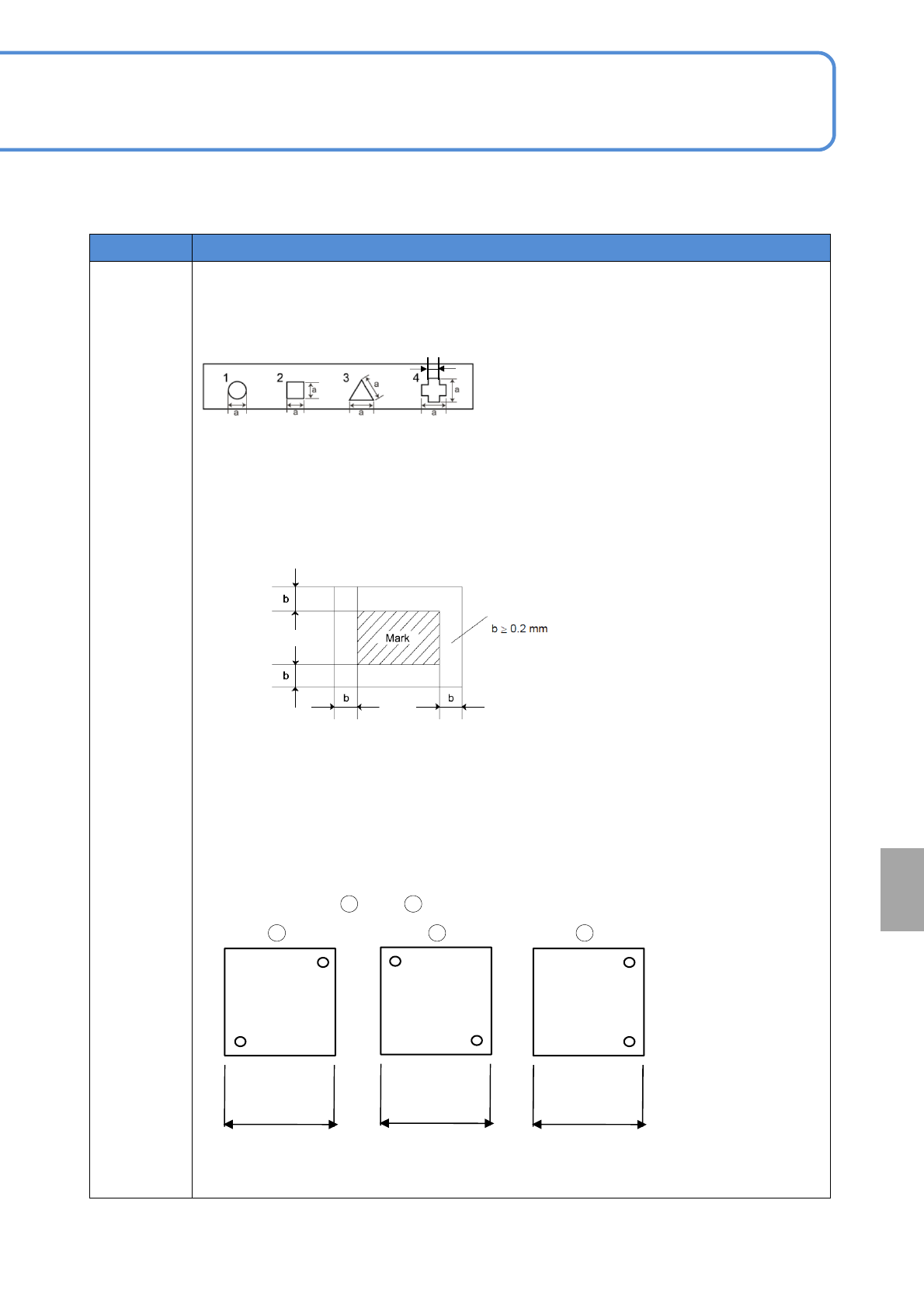
■Examples of mark shape
●PCB recognition implements compensation through the use of the physical relationship
between recognition marks and a circuit pattern.
●A fixed contrast is required between recognition marks and a PCB.
■Recognition mark dimensions and background
●The background of a mark requires the noninterference area - larger than certain
dimensions- outside the mark itself.
●Marks are not always black in color.
■Recognition mark position
●Two PCB recognition marks are required on opposing corners of a PCB.
Triangle on the 3rd figure on the left:
Equilateral triangle
Line width on 4th figure on the left:
0.3 mm or more
0.5 mm ≦ a ≦ 1.6 mm
0.3 mm ≦ c
・Recommended example
L ≦ 750 mm
We recommend and .
L
* These are example of PCB recognition mark positions. It may vary depending on
your PCB specifications.
L
L
c
1 2 3
1 2
Noninterference area