N7201A616E00_0317.pdf - 第366页
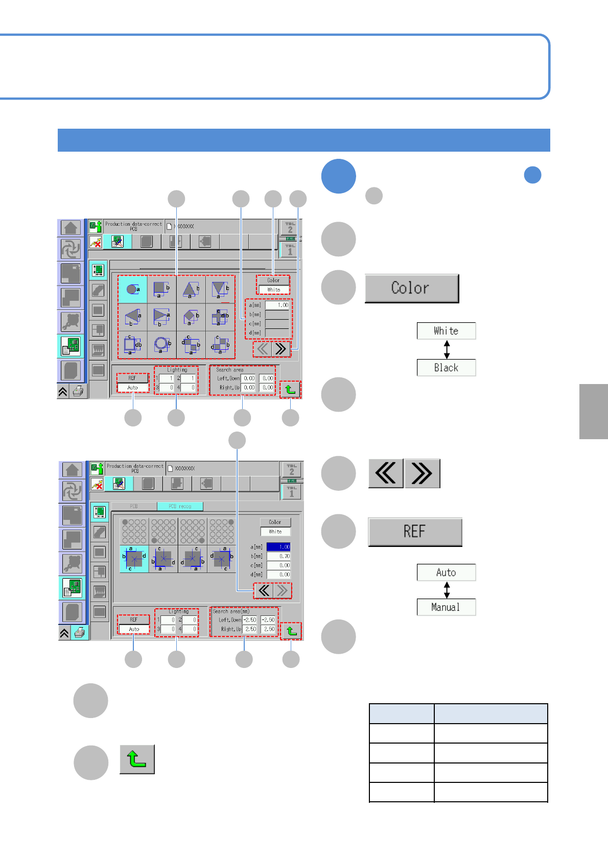
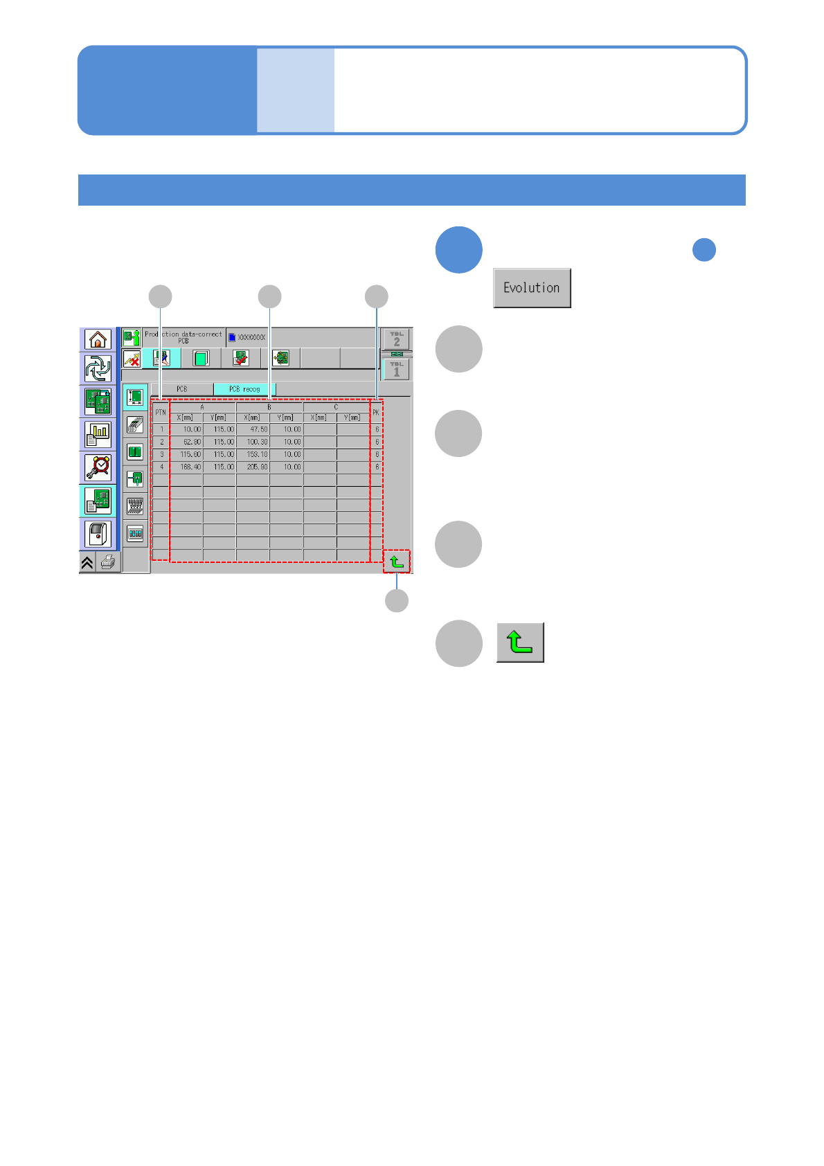
NPM-W 2 EJM7DE-MB-06O-0 0 C B PCB re cognition coor dinate of a recognition poin t (X,Y) Number to arrange several types of patte rns. A Pattern number. 6-1-3 -3 Data editing PCB r ecognition da ta edit 2 Expanded data d…
NPM-W2 EJM7DE-MB-06O-00
Lamp value of lamps 1 to 4.
6-1-3-2
B
A
C
D
Lighting
Size
Choose a recognition mark color.
E
Choose a light adjustment method.
F
Changes to the previous or next screen.
Shape selection
Search area
H
G
E F G
DA C B
Returns to the previous screen.
Shape selection and edit
Size of a selected recognition mark
shape.
●Touching the screen opens the input
window.
Recognition range of one recognition mark.
●Touching the screen opens the input window.
Choose a recognition mark shape.
H
E F G
D
H
2
By the step of (P.6-1-3-1)
1
E
(type)
●Relationship between a head camera
lighting and lighting (P.7-3-16)
Lighting Type
1 Coaxial lighting
2 High angle lighting
3 Middle angle lighting
4 Low angle lighting
Setting
change
NPM-W2 EJM7DE-MB-06O-00
C
B
PCB recognition coordinate of a
recognition point (X,Y)
Number to arrange several types of patterns.
A
Pattern number.
6-1-3-3
Data
editing
PCB recognition data
edit 2
Expanded data display
3
PK
PTN (pattern)
D
Returns to the previous screen.
Operating procedure
6-1-3
By the step of (P.6-1-3-1)
1
A B C
D
X[mm], Y[mm]
NPM-W2 EJM7DE-MB-06O-00
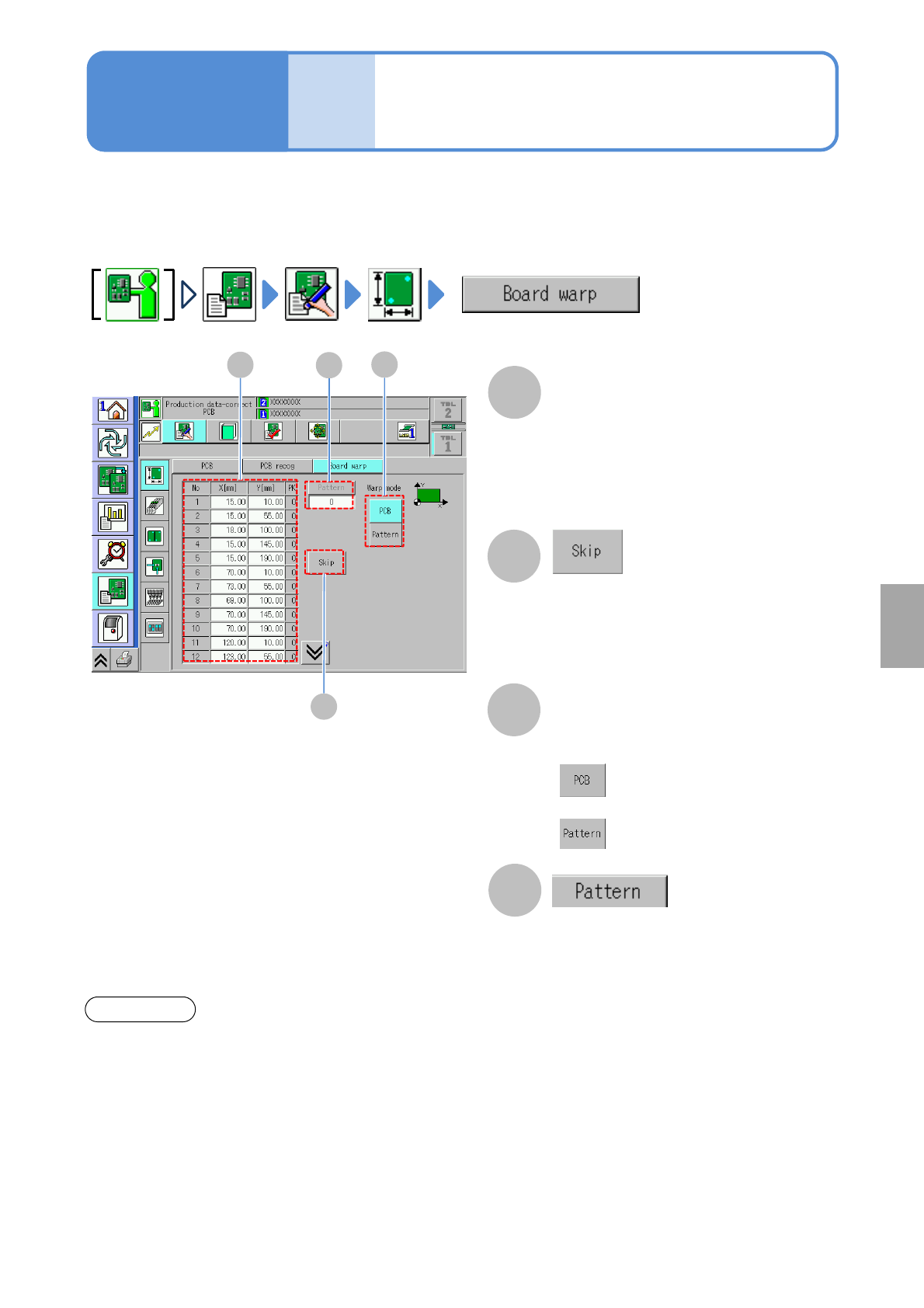
6-1-4
Data
editing
PCB warpage
measurement point data
(option)
Operating procedure
6-1-4
C
B
Skips the selected coordinates.
Select either PCB warpage or pattern
warpage.
A
C
A
Warpage mode
PCB warpage measurement
point data
D
Enables to edit coordinates.
Describes how to check and edit the PCB warpage measurement point data.
Move the cursor to the position where you change the data and enter the value.
B
D
●X[mm]:X-coordinates of measurement
point
●Y[mm]:Y-coordinates of measurement
point
●At least nine points are necessary for
measurement points
●If points are less than nine, skip is not
allowed.
:Corrects entire PCB by the
measurement result
:Correct per pattern by the
measurement result.
●Changes the display of the pattern
data (The number of registered
patterns is displayed
1,2,3・・・・・N)
●Only pattern warpage is operable.
If warpage information is transferred to the post process or received from the pre process, it is necessary to
set [PCB warpage information] on the communication switch of the production data to ‘ON’. The setting can
be confirmed on the screen. Change the setting from DGS.
Even though if the functions (such as defect pattern information, APC information) to communicate PCB
information is used, the simultaneous transfer function is available, it cannot be set on the machine. So, we
recommend you to set the function disabled. You can confirm the function for PCB information
communication by the following screen.
(→P.7-1-1)
●Receiving: Set to ON when information is received from the pre process.
●Sending: Set to ON when information is sent to the post process.
Confirmation
*Transmission of PBC warpage information between different product types is not supported. (→P.9-1-8)
Setting
change