N7201A616E00_0317.pdf - 第641页
NPM-W 2 EJM7DJ-MB-08O-00 8-1-1 -4 APC system

NPM-W2 EJM7DJ-MB-08O-00
Over-
view
Operating procedure
8-1-1
8-1-1-3
Function
■Placement position correction function
■Component inspection position correction function
The cost associated with component losses can be reduced by using the pattern skip control for the
placement or inspection heads within the line based on inspection results.
■Solder/land defect skip function
Solder inspection
standard
Variation in PCB sizes, individual PCB positions, solder printing masks or machines causes misalignment
between a solder position and a component placement position, resulting in decreasing placement quality
after reflow.
APC system controls the production line using printed all solder positions / area measurement values
together with the inspection result so that it can reduce the effects on various variations and prevent
decreasing placement quality using the following functions.
By sending (in feed-forward) data about the correction amount calculated based on the misalignment
between the position of a component placed by the placement head and the printing position of the solder
corresponding to the component to the component placement process, the component can be placed at
an optimum position with relative to the corresponding solder position.
●The amount to be corrected in X-, Y-, and A- (angle) directions is sent in feed forward.
●Solder inspection function, if the condition of solder is not conforming, stops automatic operation to allow
you locate the nonconforming solder. In addition, for a component for which measurement of the position
of the corresponding solder has failed, the correction amount of the one close to the component will be
applied, instead.
●Feed-forward control in X-, Y-, and A- (angle) directions can be set to ON /OFF on a per-component basis.
By sending (in feed-forward) the correction amount of the component placement mentioned above to the
component inspection process, misalignment of a component can be inspected based on the corrected
placement position.
By sending (in feed-forward) the correction amount calculated from the misalignment between the
positions of solder paste printed onto all lands and the ones of the respective lands* to the solder printing
process, solder paste being printed on the lands can be optimally-positioned.
For details of settings and functions, see [NPM-DGS SP data editor].
Position assuming from the PCB recognition mark measurement result
■Correction function for solder printing positions
Features 2

NPM-W2 EJM7DJ-MB-08O-00
8-1-1-4
APC
system
NPM-W2 EJM7DJ-MB-08O-00
Over-
view
Line example and APC
system 1
Operating procedure
8-1-2
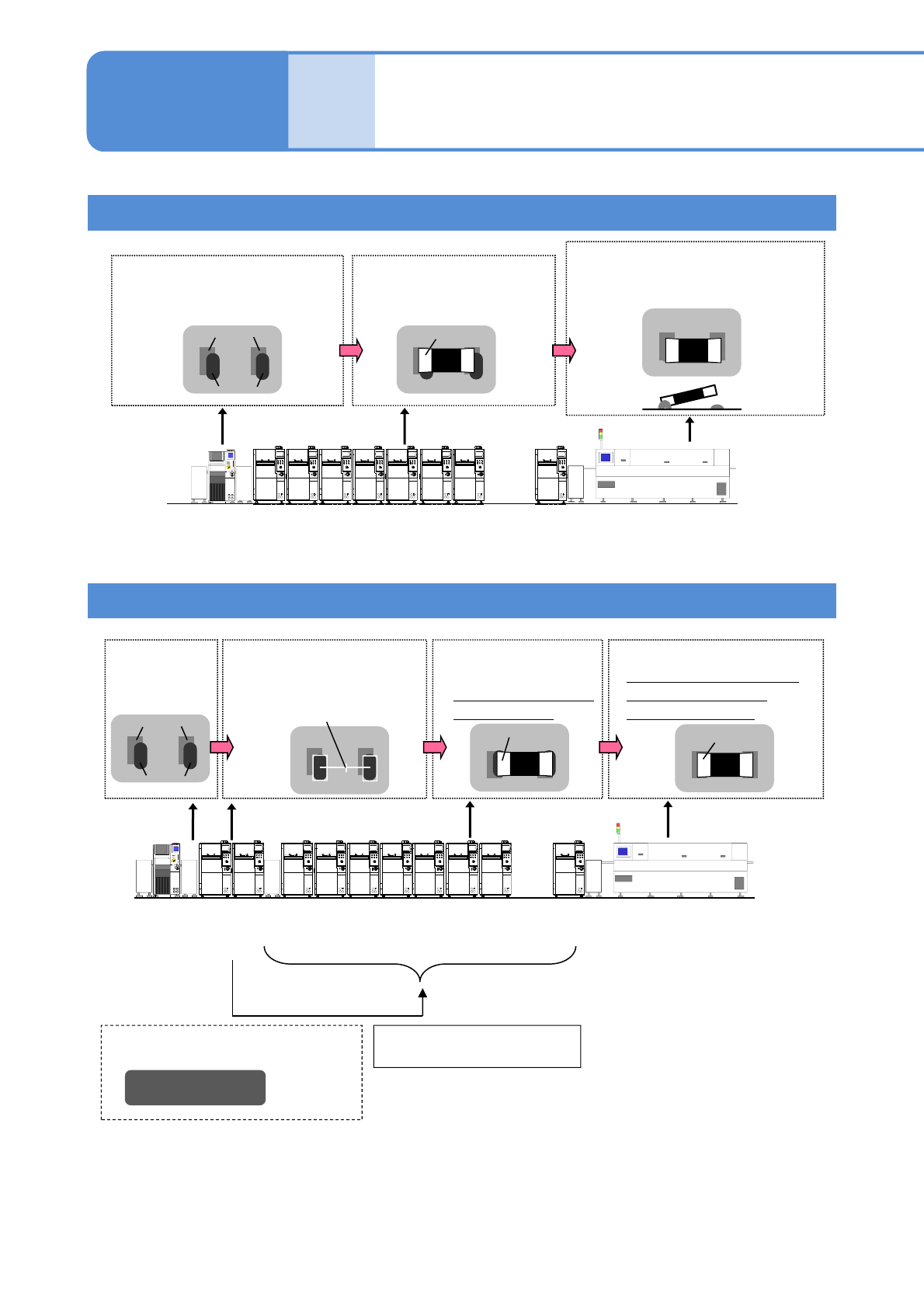
APC unsupported line example
Land
Solder
After solder printing:
Printing position misalignment
due to variations in the eland
position
After reflowing:
Nonuniform solder joint
contributes misalignment or
lifting
Part
Component placement:
Place based on the
land position
Misalignment
Lifting
APC-compliant line example (Component placement position correction)
Land
Solder
After solder
printing
Solder inspection:
Inspection and position
measurement of solder
Applicable placement
position
Part
Component
placement:
Placed based on the
solder position
After reflow:
Component moves to the
land position by self-
alignment effect
1)
Part
●Placement position correction data
●Placement skip control data
Feed-forward
communication
1) The condition of solder printing or component may disable the self-alignment.
2) An amount of correction of the placement position output from the solder inspection process is sent to
the placement / component inspection process on the downstream machine.
8-1-2-1
Solder inspection
standard
2)
・・・
Printing
Placement
Component
inspection
Reflow
・・・
Printing Placement Component
inspection
ReflowSolder
inspection