N7201A616E00_0317.pdf - 第647页
NPM-W 2 EJM7DJ-MB-08O-00 8-2-1 -2 APC system Based on co ordinate origin a nd angle obtained from PCB po sitioning mark recognition, a po sition misalignment amoun t and area differen ce from a logical value (mask gerber…
NPM-W2 EJM7DJ-MB-08O-00
8-2-1-1
System
function
details
Various functions 1
Operating procedure
8-2-1
Soldering position measurement function
■Applicable component type
Based on the coordinate origin and the angle obtained by recognizing the PCB positioning mark, the
following soldering position misalignment amount is calculated on a per-placement component basis, and
the position is corrected relative to the logical placement coordinate.
■Calculating the misalignment amount of soldering positions
dθ:
The soldering position misalignment angle averages the difference, obtained relative to all solder, between
the theoretical angle and the measurement angle of the straight line connecting two positions of solder’s
center of gravity.
Dx, dy:
The soldering position misalignment amount averages the difference between the theoretical coordinate of
solder’s center of gravity relative to all solder and the measurement coordinate taking into account the
misalignment amounting equal to the above dθ.
The most relevant placement correction amount is calculated based on the soldering position
misalignment amount and the correction amount control parameters in response to each process, and
thus components are placed to the best suited position.
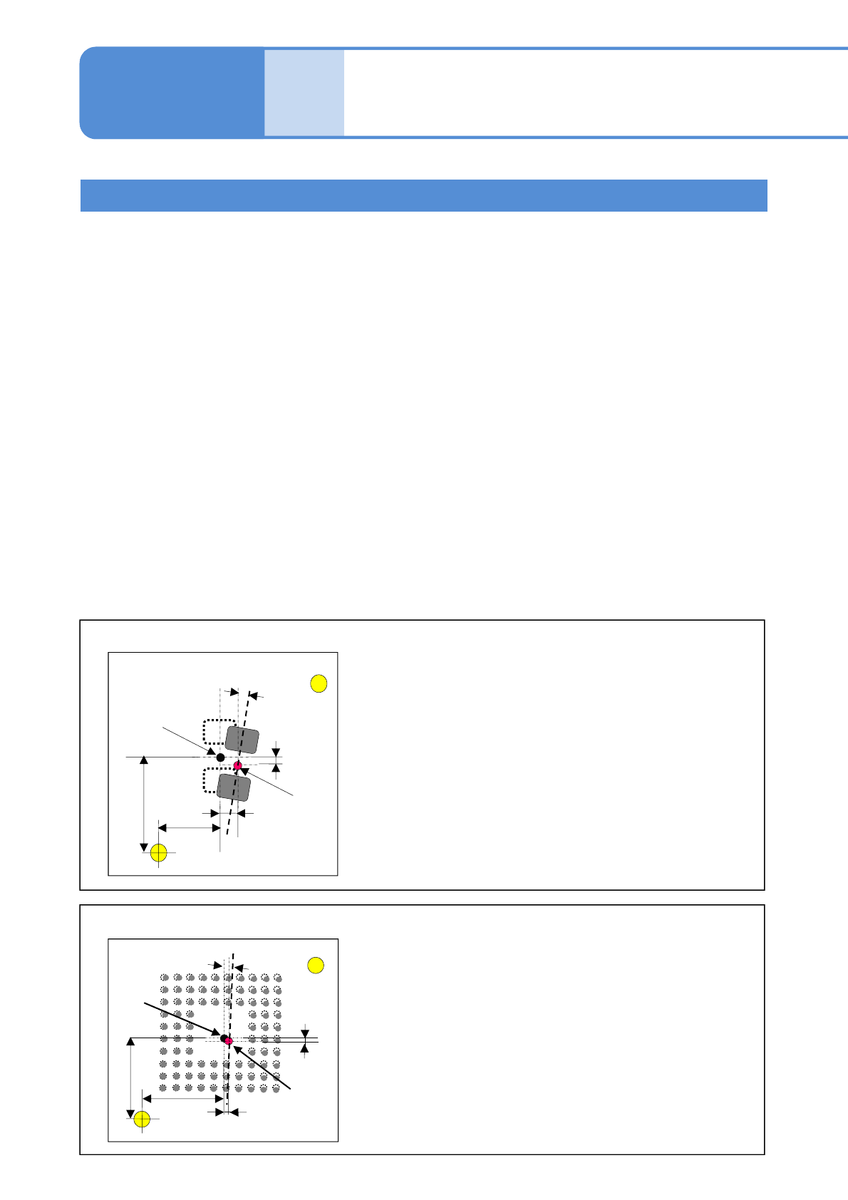
■Calculating the placement correction amount
Package component
①
⑨
③
④
⑦
⑧
⑤
⑥
②
① PCB positioning mark A
② PCB positioning mark B
③ Placement logical coordinate by positioning mark recognition
result
④ X logical coordinate of placement component
⑤ Y logical coordinate of placement component
⑥ Placement coordinate after correction
⑦ Printing misalignment amount dx of X direction
⑧ Printing misalignment amount dx of Y direction
⑨ Printing misalignment amount dx of θ direction
Square ship component
⑨
③
④
⑦
⑤
⑥
①
②
⑧
① PCB positioning mark A
② PCB positioning mark B
③ Placement logical coordinate by positioning mark recognition
result
④ X logical coordinate of placement component
⑤ Y logical coordinate of placement component
⑥ Placement coordinate after correction
⑦ Printing misalignment amount dx of X direction
⑧ Printing misalignment amount dx of Y direction
⑨ Printing misalignment amount dx of θ direction
There is no specific restriction. Specification for the solder to be measured is the same as the solder
inspection specification. See the operating instruction of the machine which performs solder inspection
(NPM inspection head or other company’s inspection machine).
1. Component placement feed forward
NPM-W2 EJM7DJ-MB-08O-00
8-2-1-2
APC
system
Based on coordinate origin and angle obtained from PCB positioning mark recognition, a position
misalignment amount and area difference from a logical value (mask gerber data of solder printing) is
calculated per mask aperture.
Dx, dy:
The difference between logical coordinates and measurement coordinates of the solder center of the
gravity is a solder position misalignment amount.
Area ratio:
Ratio [%] against the mask aperture area calculated from the gerber data is a solder area ratio.
A printing position to be corrected to the optimum solder printing position shall be the minimum
misalignment amount of solder position.
For details, see the operating instruction [NPM-DGS SP data editor] or the operating instruction of the
printer.
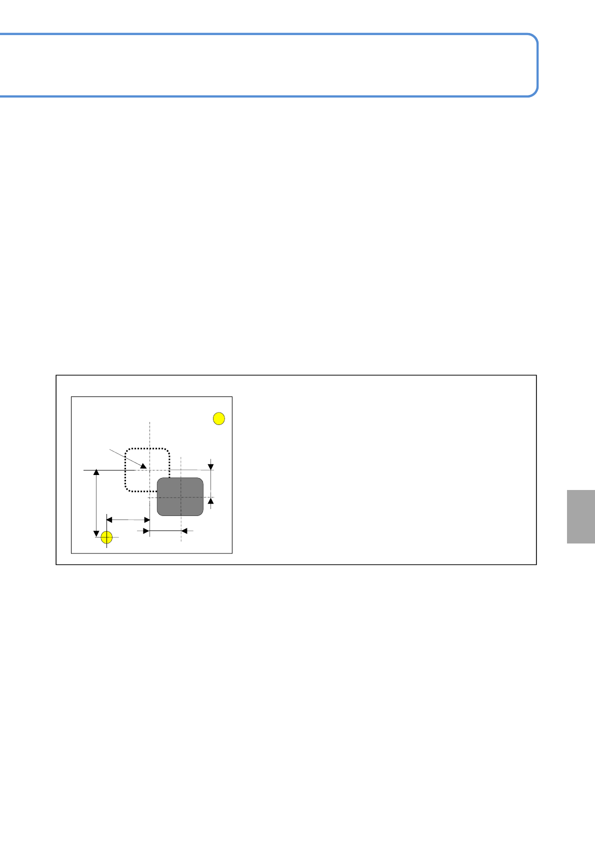
■Calculation of printing position correction amount
2. Solder printing feedback
① PCB positioning mark A
② PCB positioning mark B
③ Logical coordinates of the solder center of the gravity based
on the positioning mark recognition result
④ X logical coordinate of solder
⑤ Y logical coordinate of solder
⑥ Solder position misalignment amount dx in X-direction
⑦ Solder position misalignment amount dy in Y-direction
③
④
⑦
⑤
①
②
⑥
■Calculating a misalignment amount of soldering positions
NPM-W2 EJM7DJ-MB-08O-00
8-2-1-3
System
function
details
Various functions 2
Operating procedure
8-2-1
The placement position accuracy, not only on the surface of solder but also of flip chips placed onto the land
by fluxes or solder transfer, is intended to be improved through the feed-forward communication of the
measurement result of land positions.
Also, by inspecting the land areas and positions and then skipping the placement of all components to bad
patterns, if any, it seeks to cut down on the cost associated with component losses.
The placement standard needs to be set to “Land” in the DGS setup of detailed data on components.
By recognizing directly the land position itself where components are placed, the components can be
placed with a high degree of accuracy, providing also an appropriate response to the component
deformation as an example.
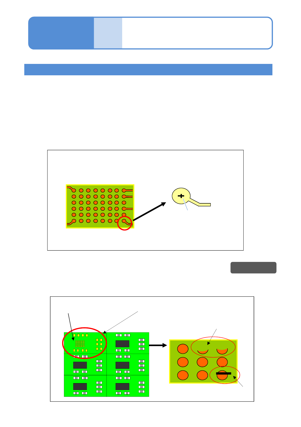
■Land position measurement function
The exclusive recognition mode, which supports the
position measurement of land with wire patterns, is
installed.
Land for flip chip
The land position is
accurately measured by the
special processing that
calculates the center from
the set shape and shape.
Land defect
Skips placement of components into the
pattern where land defects are found.
In the case where solder inspection (land) defects are found in a pattern on a multi-surface pattern board,
such as a module component, it is equipped with the function that skips the placement of any components
into the pattern.
■Solder/land inspection and defect pattern placement skip function
Land defect
Land chip
Foreign
material
Example)
Solder inspection
standard
Feed-forward function