N7201A616E00_0317.pdf - 第501页
NPM-W 2 EJM7DE-MB-06O-0 0 6-2-10 -2 Setting change Descr ibes how to check mar k re cognition when a bad mark exists o n the PCB. 3 3 4 4 When the bad mark is white White Black ● Select the mark type. When the bad mark i…
NPM-W2 EJM7DE-MB-06O-00
Produc-
tion data
teaching
Bad mark recognition
teach 1
6-2-10-1
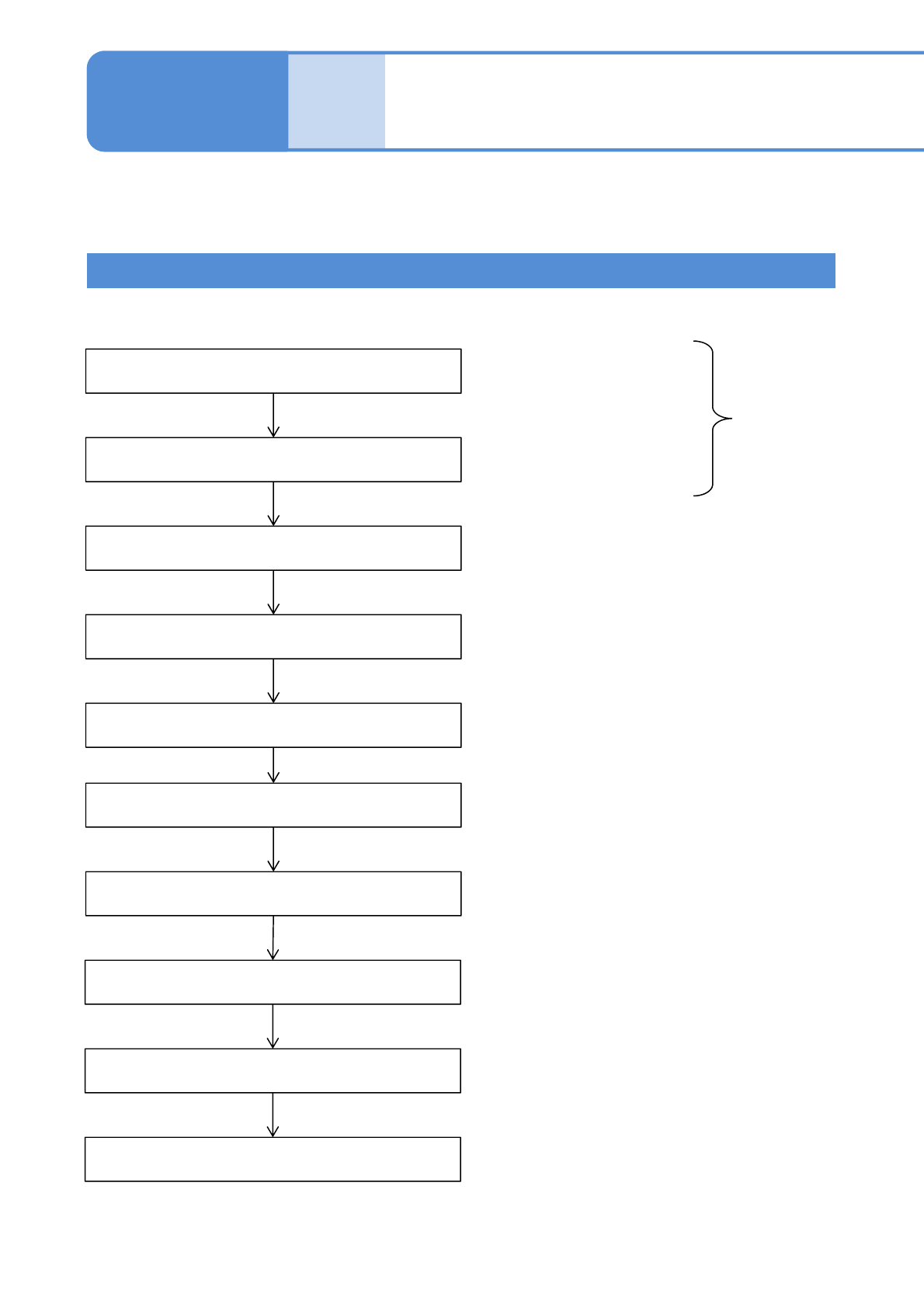
Operating procedure
6-2-10
Inputting the PCB data
Inputting the pattern attribute data
Starting the teaching
Choosing the bad mark
Setting the lamp values
Setting the area and threshold
Recognition
Saving data
To enable the bad mark recognition process, you need to turn ON the corresponding soft
switch.
Input the PCB bad mark
position (coordinates).
Input the pattern bad mark
position
Created on
NPM-DGS.
Recognition Test
Teaching is complete.
When partial defect occurs in the produced PCB in the middle of the process, if a bad
mark is put on it, you can skip placement on that pattern.
Teaching Flow
NPM-W2 EJM7DE-MB-06O-00
6-2-10-2
Setting
change
Describes how to check mark recognition when a bad mark exists on the PCB.
3
3
4
4
When the bad
mark is white
White
Black
●Select the mark type.
When the bad
mark is black
1
2
Set a PCB on the PCB entrance
+
(The PCB is loaded onto the
placement stage, and the
recognition camera moves to the
bad mark position)
2
NPM-W2 EJM7DE-MB-06O-00
Produc-
tion data
teaching
Bad mark recognition
teach 2
6-2-10-3
Operating procedure
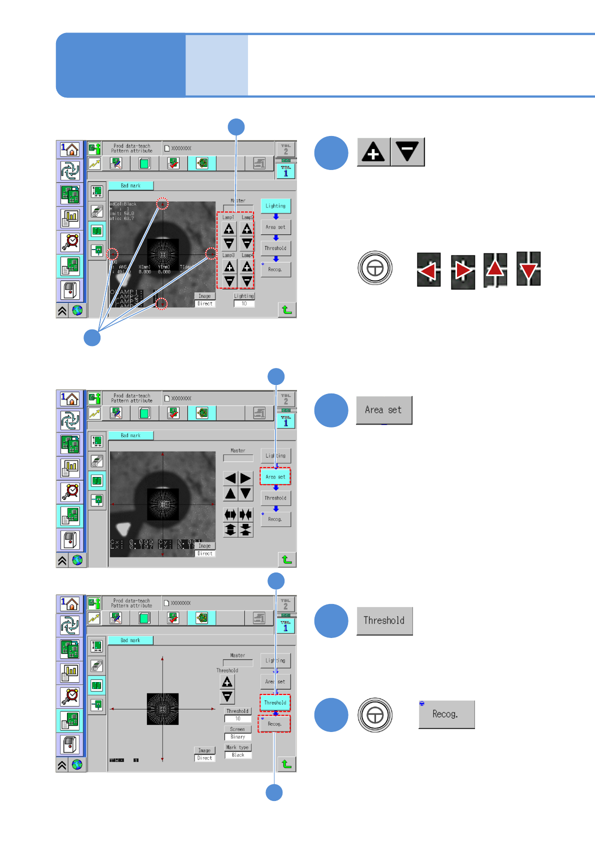
6-2-10
5
5
5
6
■When the position and the size of
recognition area are changed.
7
■When the threshold value being
recognized, screen switch or mark
type are changed.
6
8
7
+
8
After change
(Recognition is performed)
●Adjust the brightness to obtain the bad
mark. (→P.6-2-1 ‘How to adjust the
lamp value’)
■If the bad mark is not located
near the center
●Align the cross line center to the
bad mark center.
+