VI User Manual.pdf - 第202页
Tools library 7 - 40 Vision 2007 4.10 User Manual Re v 01 With Expert Mode Tick the Expert mode ( J ) to display this window. Select the ta b to edit the wa nted side of the component. Select the pin number ( A ) you wan…
Tools library
Vision 2007 4.10 User Manual Rev 01 7 - 39
7.8.4 Components leads detection
7.8.4.1 Algorithm
7.8.4.2 Parameters
Without Expert Mode
The option Expert mode (J) is not
ticked.
Select the tab to edit the wanted side of
1st component.
Select the pin number (
A
) you want to edit.
The Pitch (B) allows you to increase or
decrease the pitch size between pins.
With Offset all leads position (C) you
can modify the offset of all leads.
Tick Apply to all sides (D) to apply
these modifications to all sides.
Click on Display (E) button to see
modifications in the image window.
Increment (F) determine the value of
increase (or decrease) of pitch and off-
set of leads.
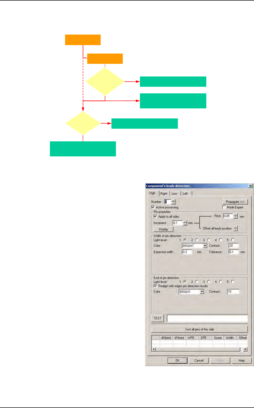
Missing lead
Yes
All pins are
missing ?
Missing component
Yes
Return fine X, Y, Theta
of the component
No
Return fine X, Y, Theta
of the lead for joint realignment
For each pin
For each side
Width
& end of lead
detection
fails ?
Custom
Tools library
7 - 40 Vision 2007 4.10 User Manual Rev 01
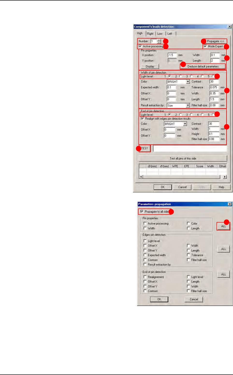
With Expert Mode
Tick the Expert mode (J) to display this
window.
Select the tab to edit the wanted side of
the component.
Select the pin number (
A
) you want to edit.
For the selected pin of the selected side,
tick
Active processing
(
B
) to run the
detection and select the
Light level
(
C
).
In Pin properties (D) section, enter the
features of the selected pin. Ensure
changes to adapt the model to reality. If
you change any parameters, press De-
duce default parameters (E) button to
change automatically the linked treat-
ments (solder joints and bridge detec-
tion).
In Edges pin detection (F) section,
enter the various parameters.
In End of pin detection (G) section,
enter the various parameters.
Press TEST (H) button to test of the
selected pin.
When you click on Propagate >>> ( I )
button, in order to propagate the different
parameters to all the sides, the opposite
window appears.
Tick Propagate to all sides (1) to propa-
gate the ticked parameters to all sides of
the component. Otherwise they will be
propagated to all pins of the selected
side.
Click on ALL button (2) to tick or not all
the parameters from the section.
A
B
D
E
F
G
I
H
J
C
C
1
2
Custom
Tools library
Vision 2007 4.10 User Manual Rev 01 7 - 41
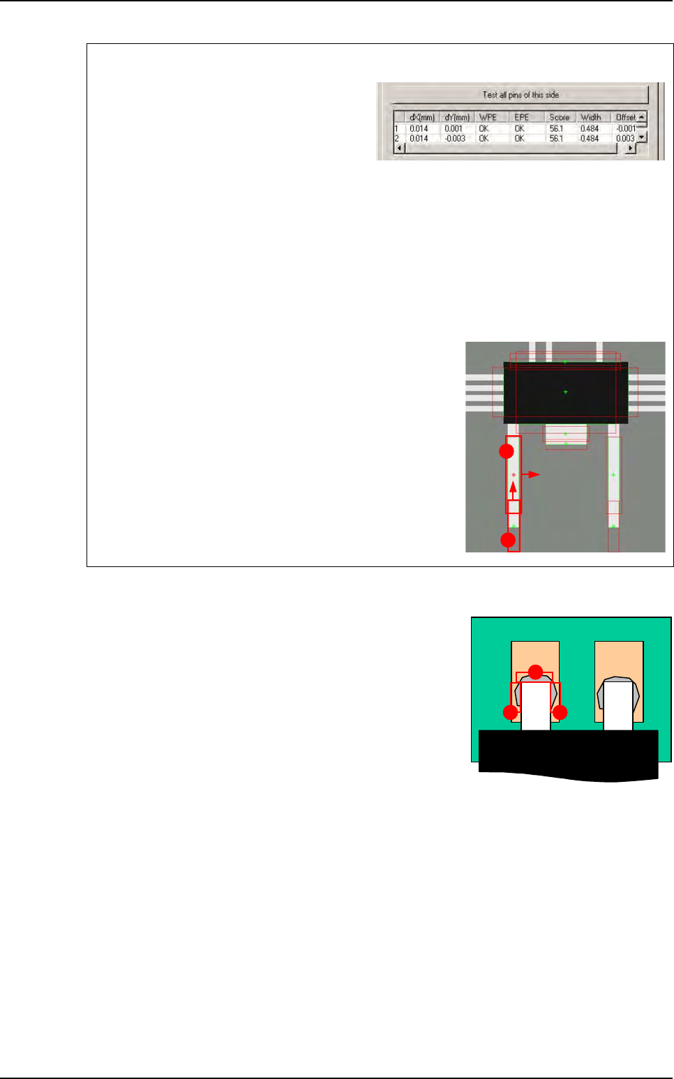
7.8.5 Solder joints detection
We can detect this flux by placing histograms in top of the
solder joint. There are 3 locations around the lead where the
weld could be inspected:
A End of lead,
B Right side,
C Left side.
One side test
Click on Test all pins of this area button to
test all the pins of one side.
dX & Y(mm): lead position deviation.
WPE: success of the edge for the width de-
tection.
EPE: success of the edge for the end of lead detection.
Score: average of the 2 scores.
Width: width computed by the double Edge.
Offset: lateral offset of the double edge from the center of the edge window.
Test results
A
Edges pin detection: edge double.
B End of pin detection: simple edge.
A
B
A
BC
Custom