CP45-英文版培训教材.pdf - 第46页
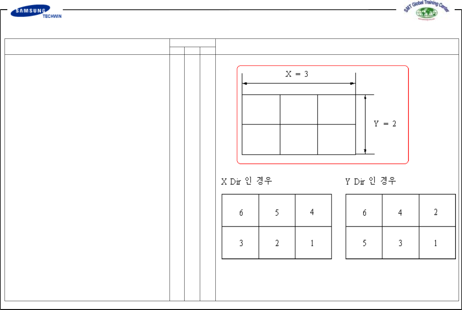
Operating Manual MODEL Reference Figure CP-45/55 Operation Process -> <Number> Edit Box Area T oe n t e rt h en u m b e ro fA r r a yP C B as follows. (X:3, Y:2) -> <Count Direction> Option Button Area …
Operating Manual
MODEL
Reference Figure
CP-45/55 Operation Process
V
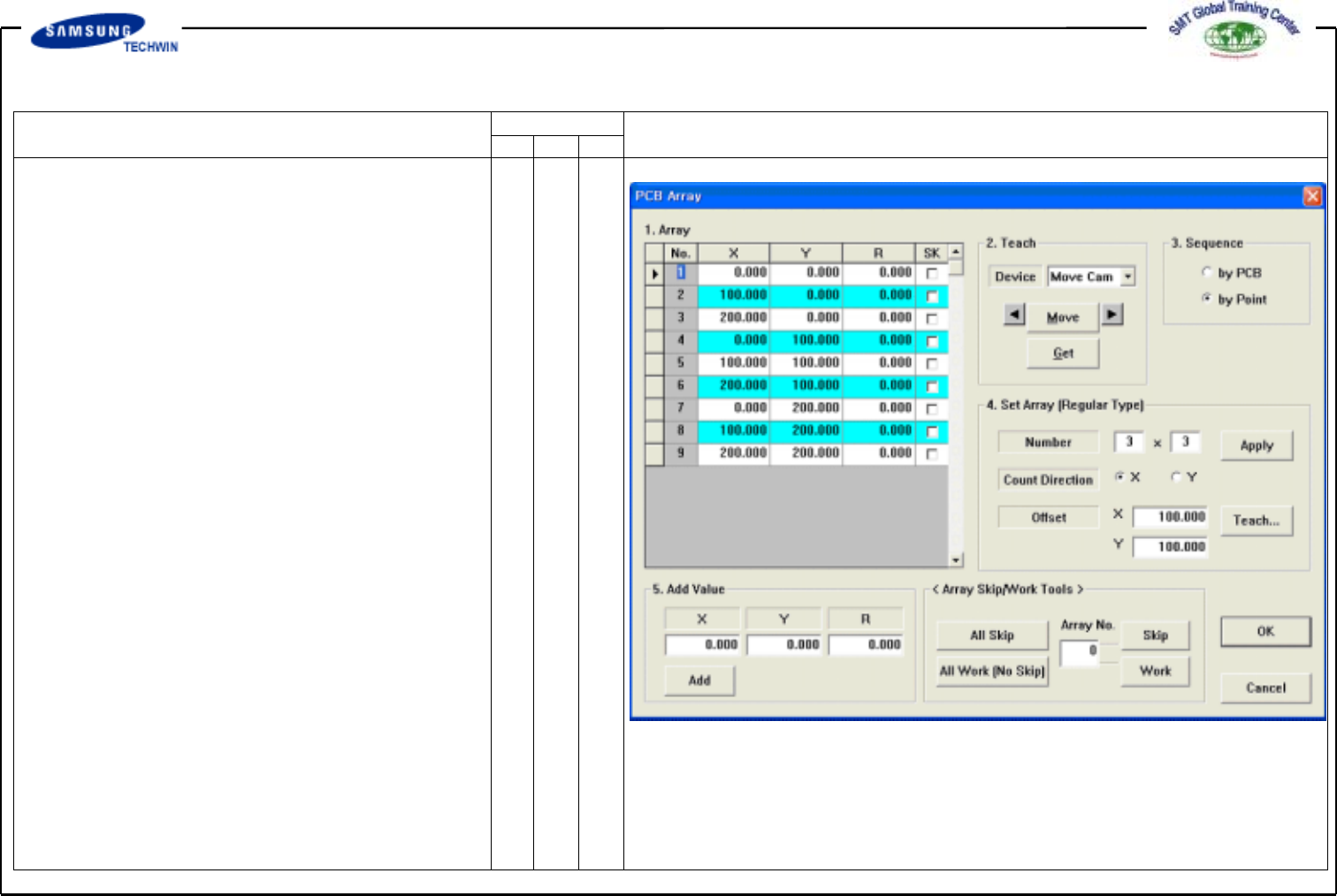
<Array…> Button
Now we will register PCBs more
than one, i.g. boards are arrayed
with total 9 boards of X:3 and Y:3.
If you click this button, Dialogue
Box as shown in the right will be
displayed.
^ <1. Array> Area
^ To set the offset value of Array
PCB Origin for "Place Origin" of
PCB Board. Check that reference
points by each board are identical.
^ <2. Teach> Area
To move Device XY, R drive shaft
to the defined position or to obtain
the current position of XY, R drive
shaft.
^ <4. Set Array (Regular Type)>Area
To setup the Array PCB.
Offset value of individual Array
PCB will be set automatically by
this function when the place
condition of Array PCB is regular.
Operating Manual
MODEL
Reference Figure
CP-45/55 Operation Process
-> <Number> Edit Box Area
ToenterthenumberofArrayPCB
as follows. (X:3, Y:2)
-> <Count Direction> Option Button Area
To select the counting method of
Array PCB Number. (Give a priority
to X Direction)
-> <Offset> Edit Box Area
This value is to automatically set
the offset value of Array PCB Origin.
Enter the moving offset of the basic
board and X and Y axes boards.
Operating Manual
MODEL
Reference Figure
CP-45/55 Operation Process
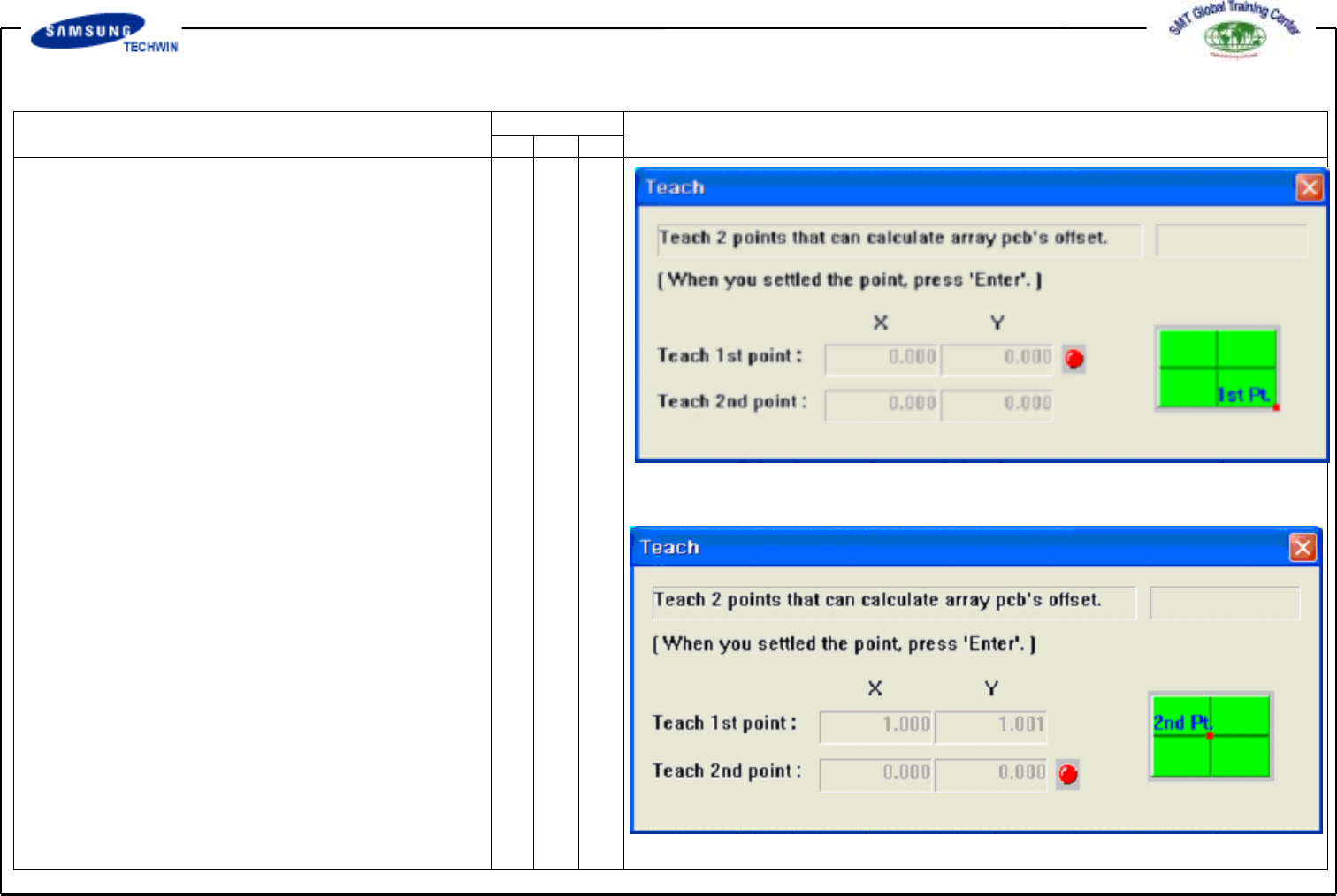
Fig. 01. Screen of Array PCB Offset 1st Point Teach
Fig. 02. Screen of Array PCB Offset 2nd Point Teach
-> <Teach> Button
This button is to teach the Array
PCB offset value with the teaching
method identical to that of PCB size.
If you click this button, the
following screens will be displayed
in sequence.
Teach the 1st origin point of Array
PCB. If you press the "Enter" Key
after teaching, a screen as shown
in Fig. 2 will be displayed. Teach
the origin point on position allowing
to determine the offset.
After teaching, if you press the
"Enter" key, the following screen
(Fig. 3) will be displayed.
If you press the “Enter” key,
teaching work of Array PCB Offset
Value will be finished.