00197498-03_UM_SiplaceCA-Serie_EN.pdf - 第198页
3 Technical Data User Manual SIPLACE CA-Series 3.15 PCB Warpage From software version SC.708.0 Edition 12/2014 EN -DRAFT 198
User Manual SIPLACE CA-Series 3 Technical Data
From software version SC.708.0 Edition 12/2014 EN -DRAFT 3.15 PCB Warpage
197
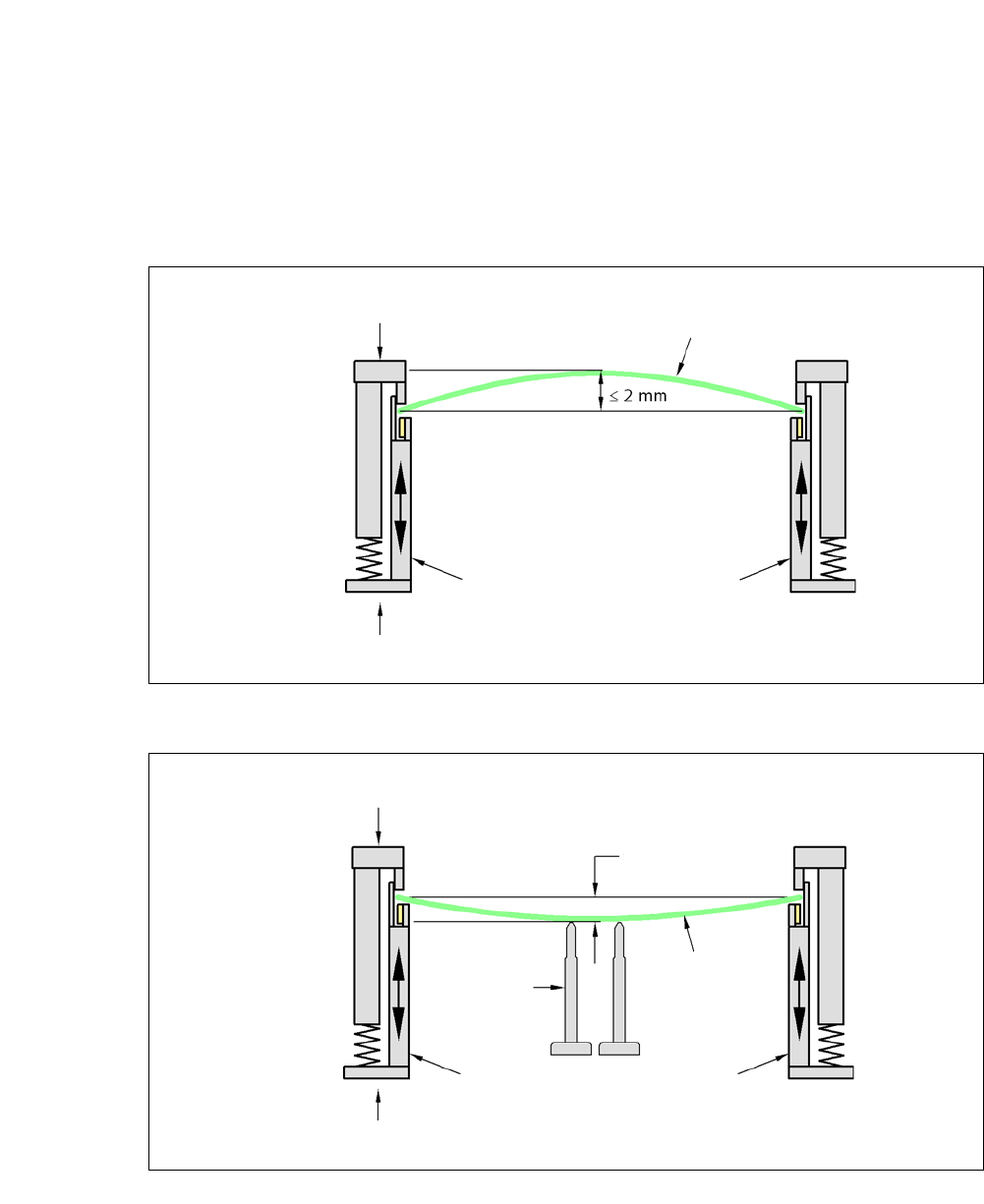
3.15.0.2 PCB Warpage During Placement
A warpage of 2 mm could lead to problems focusing on local fiducials and ink spots in the middle
of the PCB. The digital camera's focus is 2 mm. When all the tolerances are taken into account,
this value is reduced to 1.5 mm. Also note that the component height is reduced by the warpage.
3
3
PCB warpage down, max. 0.5 mm
3
Use magnetic pin supports to achieve this value.
Movable clamping device
Fixed clamped edge
Printed circuit board
Conveyor side
Printed circuit board
Magnetic pin
support
Movable clamping device
Fixed clamped edge
Conveyor side
0.5 mm

3 Technical Data User Manual SIPLACE CA-Series
3.15 PCB Warpage From software version SC.708.0 Edition 12/2014 EN -DRAFT
198
User Manual SIPLACE CA-Series 4 SIPLACE Wafer System (SWS)
From software version SC.708.0 Edition 12/2014
199
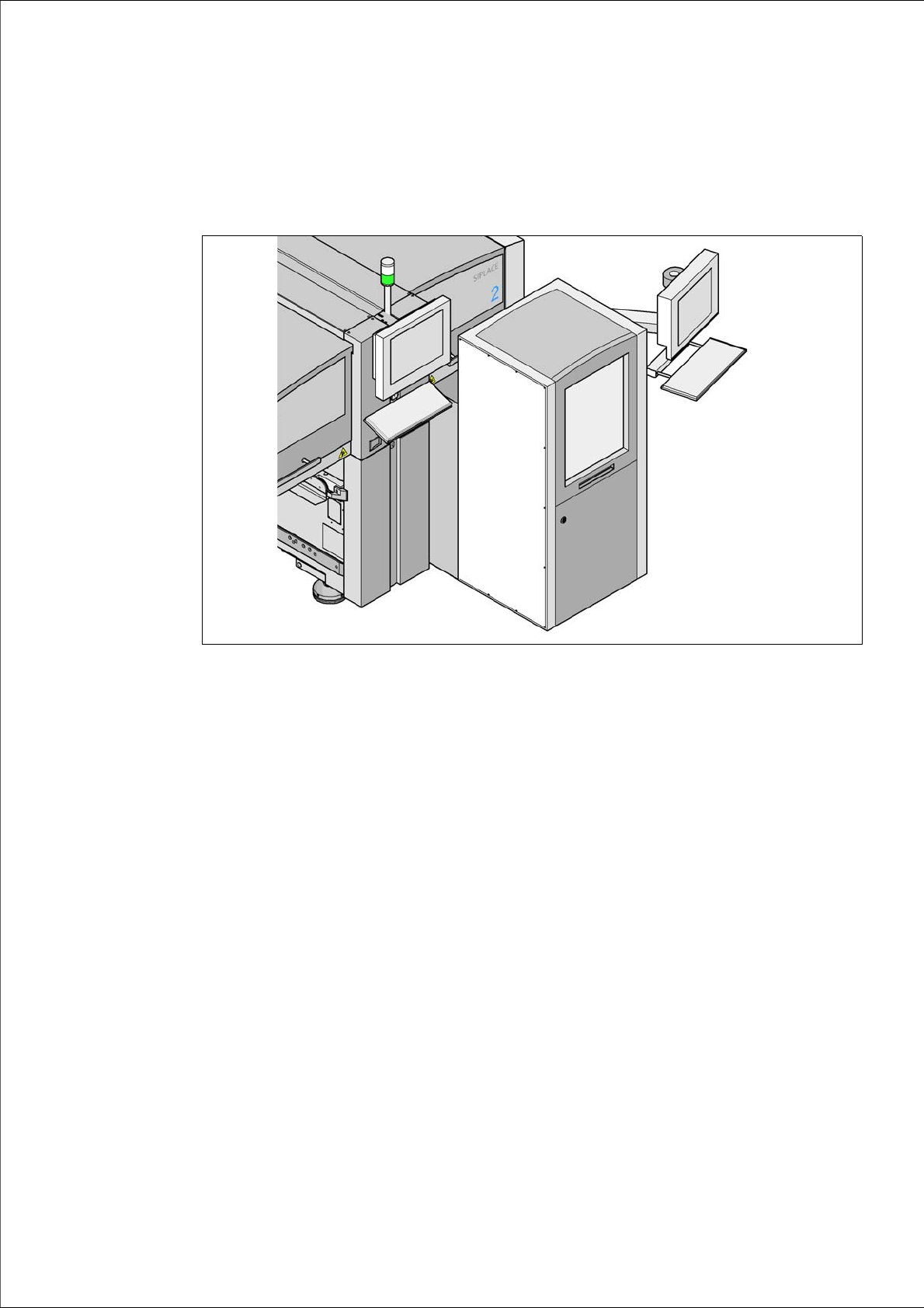
4 SIPLACE Wafer System (SWS)
4
Fig. 4.0 - 1 SWS at location 2 of SIPLACE CA4