00197498-03_UM_SiplaceCA-Serie_EN.pdf - 第206页
4 SIPLACE Wafer System (SWS) User Manual SIPLACE CA- Series 4.1 Functions From software version SC.708.0 Edition 12/2014 206 4 Fig. 4.1 - 5 Step s in the Embedded Wafer Level Ballgrid Array process (1) Laminate thermal r…

User Manual SIPLACE CA-Series 4 SIPLACE Wafer System (SWS)
From software version SC.708.0 Edition 12/2014 4.1 Functions
205
4.1.3.5 Pickup Process
During the pickup process, the die is transferred to the tool or to the nozzle of the flip unit. The flip
unit transfers the die on it either to the placement head (flip chip process) or to the die attach unit
(die attach process).
The die attach unit rotates the die again and then presents it to the placement head.
The following equipment is required for this step:
Flip Unit
Die Attach Unit (optional)
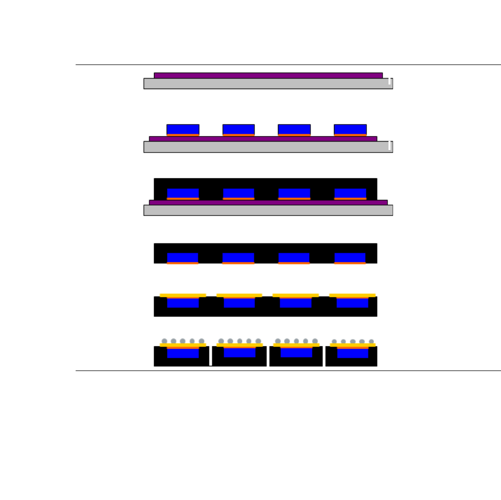
4.1.4 Embedded Wafer Level Ballgrid Array (eWLB/WLFO) Process
Embedded Wafer Level Ball Grid Array is a packaging technology which allows you to produce
thin components with excellent electrical conduction, using a chip fan out solution. This means
that the area used for the connection pads is larger than the actual silicium, thereby creating con-
tact distances suitable for SMD.
For this process, the chip components are placed with the active surface face down on a carrier
with double-adhesive foil. This structure is molded after placement. After the die bonding process
on the carrier, wafer structuring processes are used to create the electrical contacts. The mold
area around the silicium is used as the carrier for the "conductive paths" (fan out). The compo-
nents are then tested, labeled and packaged i.e. in tapes.
4 SIPLACE Wafer System (SWS) User Manual SIPLACE CA-Series
4.1 Functions From software version SC.708.0 Edition 12/2014
206
4
Fig. 4.1 - 5 Steps in the Embedded Wafer Level Ballgrid Array process
(1) Laminate thermal release tape on the metal carrier
(2) Make sure that the active side to be placed by the wafer (Flip Chip) faces down onto the
thermal release tape
(3) Molding under pressure; hardening at 150°C
(4) Release
(5) Re-Distribution Layer (RDL)
(6) Balling & single
(7) Testing, labeling, packing
1
2
3
4
5
6
User Manual SIPLACE CA-Series 4 SIPLACE Wafer System (SWS)
From software version SC.708.0 Edition 12/2014 4.1 Functions
207
4.1.5 Pick & Transfer Process in Detail
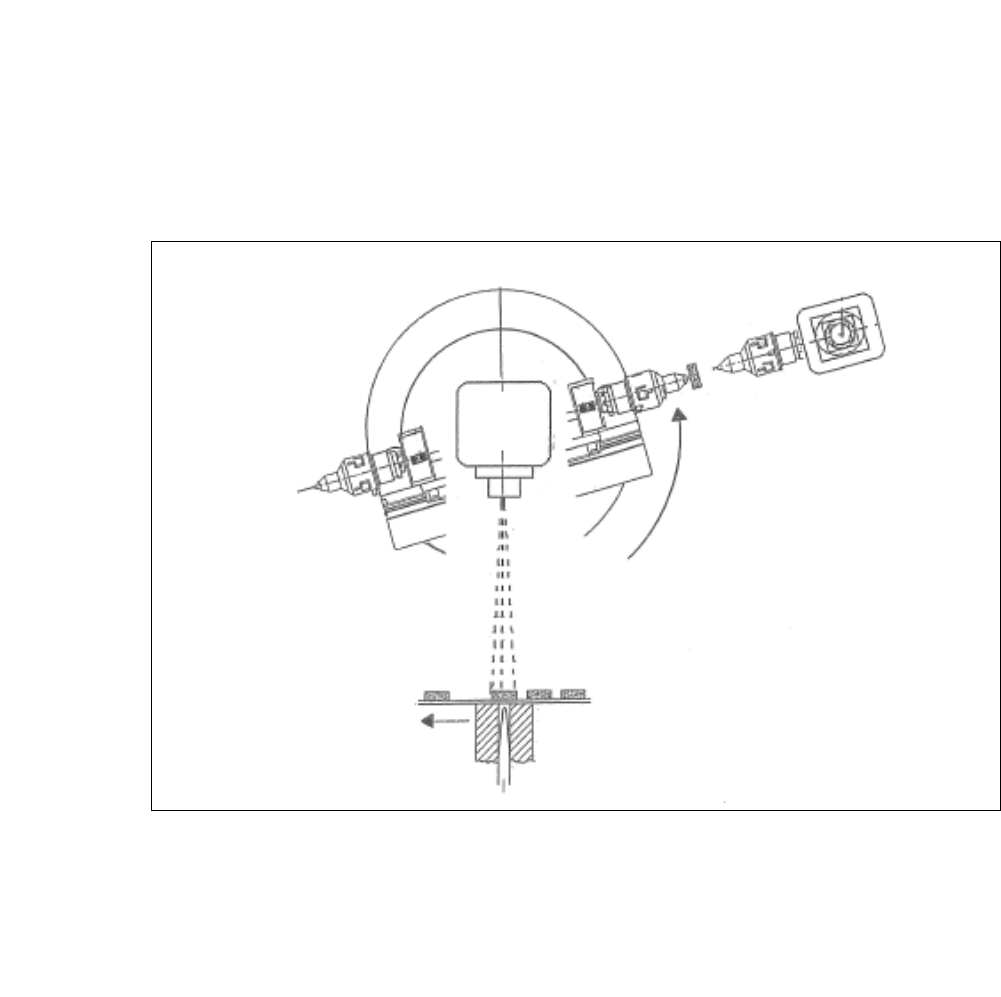
4.1.5.1 Flip Chip Segment 1 (Nozzle)
4
Fig. 4.1 - 6 Flip Chip Segment 1 (Nozzle)
(1) The wafer X-Y travels to the next chip
(2) The flip chip rotary unit segment 1 turns to the handover position "Die Attach".
During the rotation (from the camera "free Position") the picture recognition of the next chip
is carried out. 4
Wafer
Camera