00195941-03-UM SiplaceCA-EN.pdf - 第179页
User Manual SIPLACE CA 3 Technical Data Edition 08/2011 EN 3.7 SIPLACE Wafer System (SWS) 179 3.7.7.2 Die Att ach Unit 3 Fig. 3.7 - 29 Die attach unit (1) Motor for rot ating the die attach un it (2) Driver (3) Motor tra…
3 Technical Data User Manual SIPLACE CA
3.7 SIPLACE Wafer System (SWS) Edition 08/2011 EN
178
3.7.7 Options
3.7.7.1 Linear Dipping Unit (LDU)
3
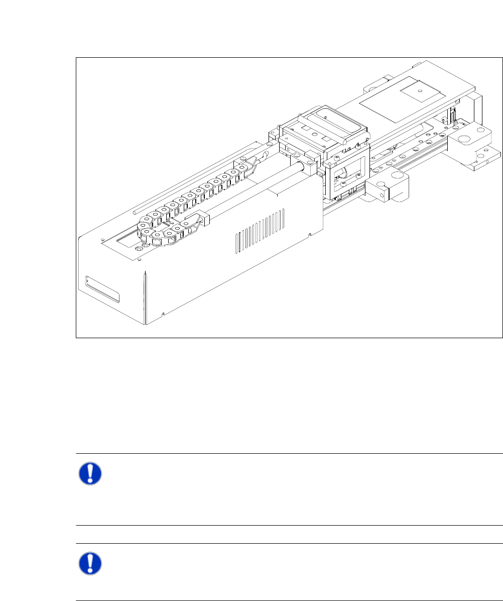
Fig. 3.7 - 28 Linear Dipping Unit (LDU)
The linear dipping unit (LDU, Linear dipping unit) is used frequently, to apply the flux on the die
during the flip chip process. This is necessary in order to ensure the reflow process.
The LDU is able to apply high-precision layers of flux. This flux is made available in a so-called
cavity. The depth of the cavity determines the thickness of the flux layer.
NOTE 3
Basically, the LDU has to be supplied for all types of appropriate flip chip fluxes.
However, Epoxid and solder pastes should only be used after performing in-house tests!
NOTE 3
The LDU cannot be used in conjunction with the die attach unit.
User Manual SIPLACE CA 3 Technical Data
Edition 08/2011 EN 3.7 SIPLACE Wafer System (SWS)
179
3.7.7.2 Die Attach Unit
3
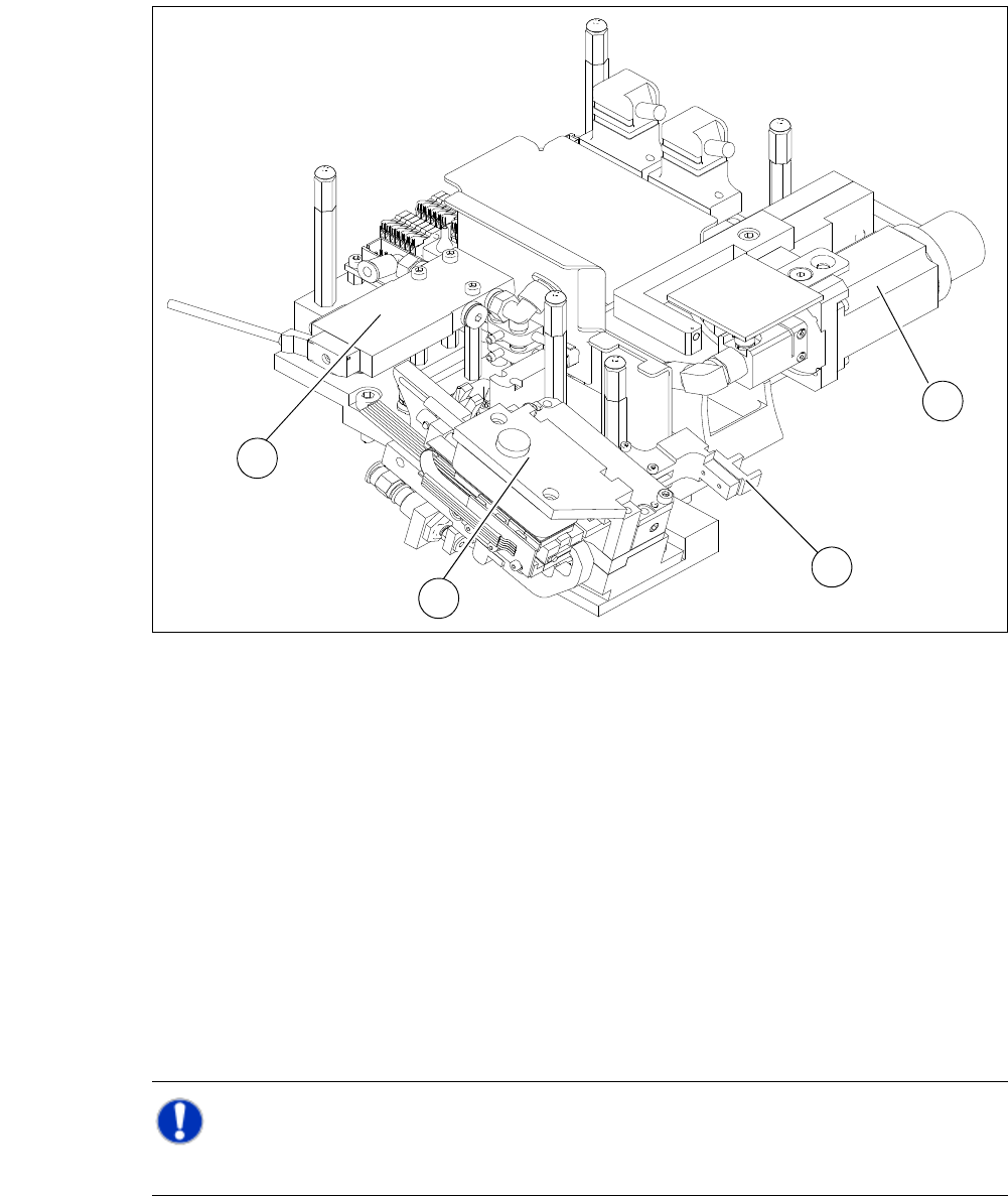
Fig. 3.7 - 29 Die attach unit
(1) Motor for rotating the die attach unit
(2) Driver
(3) Motor transfer X axis
(4) Solenoid valve
The die attach unit is used for the die attach mode.
The flip unit hands the die over to the die attach unit. The die attach unit rotates the die appropri-
ately and provides it for pickup. The die is provided to the placement head in the same top-bottom
orientation as on the wafer and is also placed in this orientation.
In die attach mode only one nozzle of the flip unit is used. The flip unit picks up the next die while
the current die is being picked up by the placement head on the die attach unit.
NOTE 3
The die attach unit cannot be used in conjunction with the LDU.
1
2
3
4

3 Technical Data User Manual SIPLACE CA
3.7 SIPLACE Wafer System (SWS) Edition 08/2011 EN
180
3.7.7.3 Small Die Kit
The small die kit is used when dies smaller than 1 mm have to be processed. It is available as an
option and consists of the following modules:
– A high-resolution camera system
– A small die ejector tool
– A component sensor
3.7.7.4 Wafer Map System
Wafer mapping is increasingly becoming a standard function in die placement processes. The wa-
fer map assigns every die on the wafer his function class.
The function class could simply be "good" or "bad". However, up to 255 classes can be assigned
to describe the die properties in detail.
Firstly, the SWS needs to identify the wafer. Normally, this involves reading in the barcode on the
wafer frame. This wafer ID is then used to select the required wafer file on the wafer map server.
In a second step, the abstract die ID from the wafer map file (column/row) is set in relation to the
real position of the die on the wafer. This position can be calculated by identifying special refer-
ence dies on the wafer and by determining the wafer center.
NOTE 3
The calculation of positions with the help of the wafer edge recognition function only works reli-
ably for dies which are 3 mm or larger.
The wafer map function is primarily a software option. This option includes a server system for
wafer map files with a conversion of customer-specific wafer map standards to the SWS standard.
The SIPLACE CA uses the "ALPS" OEM system as wafer map server and data transmission sys-
tem.