00195941-03-UM SiplaceCA-EN.pdf - 第181页
User Manual SIPLACE CA 3 Technical Data Edition 08/2011 EN 3.7 SIPLACE Wafer System (SWS) 181 3.7.7.5 Barcode Scanner The barcode scanne r at the SWS reads t he barcode attached to th e wafer frame. 3 Fig. 3.7 - 30 Barco…

3 Technical Data User Manual SIPLACE CA
3.7 SIPLACE Wafer System (SWS) Edition 08/2011 EN
180
3.7.7.3 Small Die Kit
The small die kit is used when dies smaller than 1 mm have to be processed. It is available as an
option and consists of the following modules:
– A high-resolution camera system
– A small die ejector tool
– A component sensor
3.7.7.4 Wafer Map System
Wafer mapping is increasingly becoming a standard function in die placement processes. The wa-
fer map assigns every die on the wafer his function class.
The function class could simply be "good" or "bad". However, up to 255 classes can be assigned
to describe the die properties in detail.
Firstly, the SWS needs to identify the wafer. Normally, this involves reading in the barcode on the
wafer frame. This wafer ID is then used to select the required wafer file on the wafer map server.
In a second step, the abstract die ID from the wafer map file (column/row) is set in relation to the
real position of the die on the wafer. This position can be calculated by identifying special refer-
ence dies on the wafer and by determining the wafer center.
NOTE 3
The calculation of positions with the help of the wafer edge recognition function only works reli-
ably for dies which are 3 mm or larger.
The wafer map function is primarily a software option. This option includes a server system for
wafer map files with a conversion of customer-specific wafer map standards to the SWS standard.
The SIPLACE CA uses the "ALPS" OEM system as wafer map server and data transmission sys-
tem.
User Manual SIPLACE CA 3 Technical Data
Edition 08/2011 EN 3.7 SIPLACE Wafer System (SWS)
181
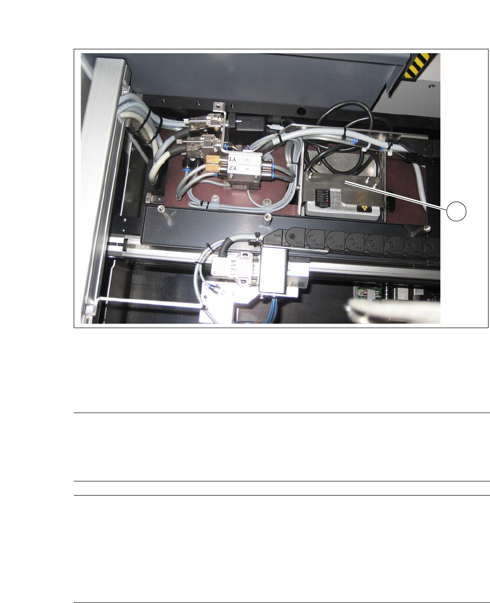
3.7.7.5 Barcode Scanner
The barcode scanner at the SWS reads the barcode attached to the wafer frame.
3
Fig. 3.7 - 30 Barcode scanner - installed in the wafer changer in this example
(1) Barcode scanner
3.7.8 Technical Data
1
Board size
Length 50 mm to 610 mm
Width 50 mm to 508 mm
Thickness 0.3 mm to 4.5 mm
Curvature Up to 0.5 mm
Board types PCB, FR4, BGA, Boat, Leadframe
SIPLACE Wafer System
Placement method Flip chip, die attach
Die size 0.8 mm x 0.8 mm up to 12 mm
(larger dies on request)
Die thickness 0,05 mm to 4 mm
Wafer size up to 12"
Frame size up to 15"
Wafer cassette max. 25 slots
3 Technical Data User Manual SIPLACE CA
3.8 Placement Heads Edition 08/2011 EN
182
3.8 Placement Heads
NOTE 3
A Twin head can only be used in a placement area without SWS.
NOTE 3
The C&PCA heads differ from conventional C&P heads primarily in their enhanced accuracy.
which is accomplished by a selection process.
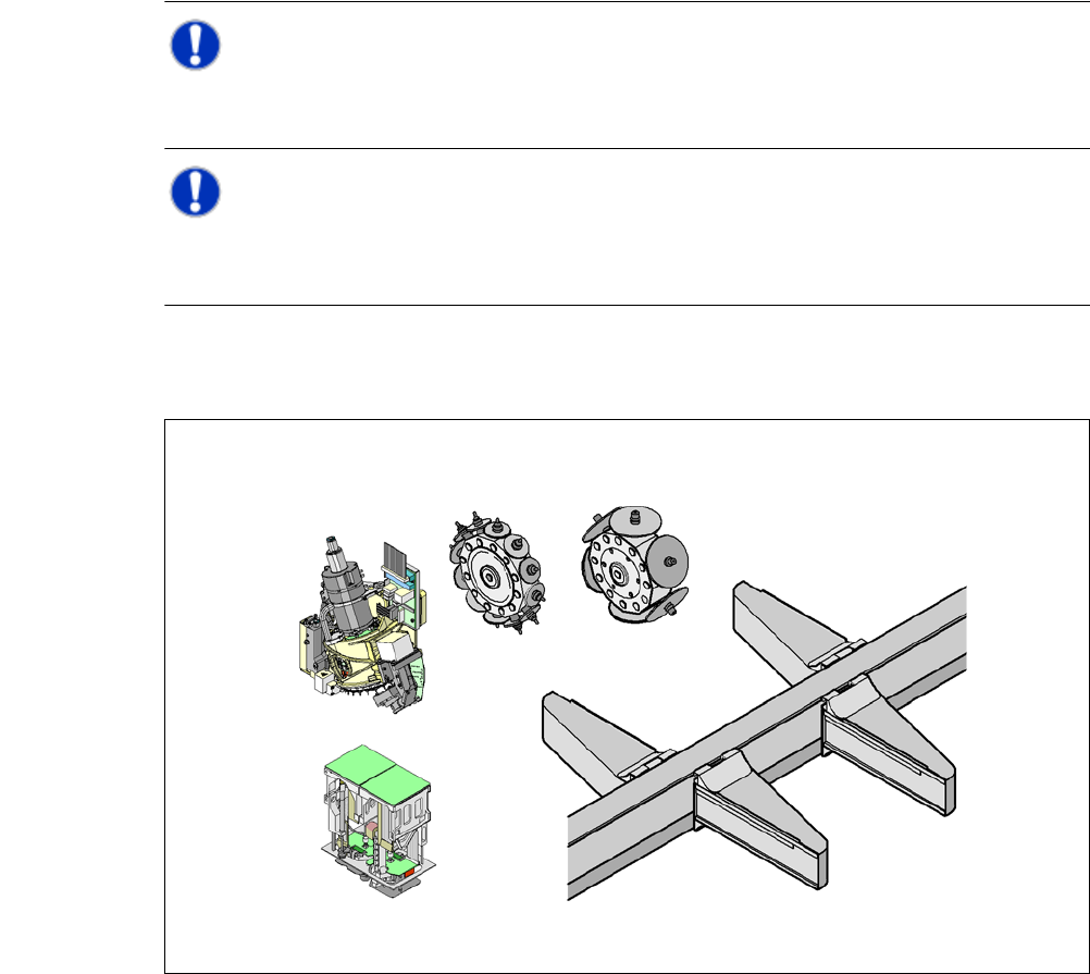
3.8.1 Placement Head Configurations for CA4 Placement Machines
3
Fig. 3.8 - 1 Placement head configuration - SIPLACE CA4
C&P12CA
C&P6CA
Placement area 2
G1
G2
G3
G4
C&P20CA/C&P12CA/
C&P6CA/TH
C&P20CA/C&P12CA/
C&P6CA/TH
C&P20CA/C&P12CA/
C&P6/TH
C&P20CA/C&P12CA/
C&P6CA/TH
C&P20CA
Placement area 1
TH