JX-350_EPU使用说明书.pdf - 第69页
EPU Instruction M anual C hapter 4 Creating a Production Progr am 4- 21 12) Bad mark position Select the “ Not Used ” radio button or t he “ Used ” radio button depending on whether a bad mark is used or not. W hen you s…
EPU Instruction Manual Chapter 4 Creating a Production Program
4-20
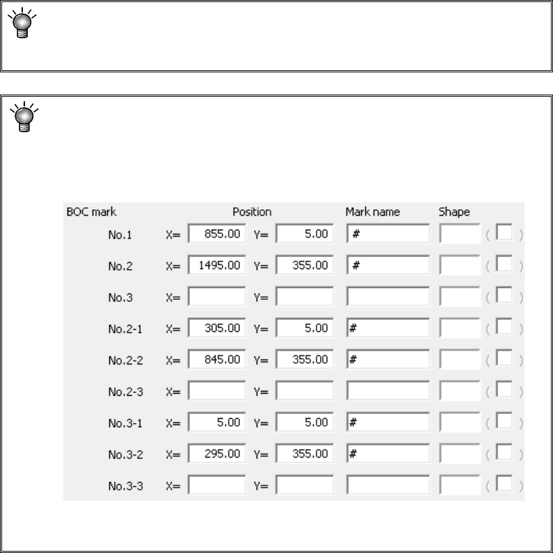
This is the distance from the PWB origin if "PWB marks are used" has been
selected, or the distance from the circuit origin if "Circuit marks are used"
has been selected as the "BOC type" on the "Basic setting" screen.
For using a long PWB:
For a large-shaped PWB whose external length X exceeds 650mm, set the
first and second BOC marks; for an optional large-shaped PWB whose
external length X exceeds 1200mm, set the first, second and third BOC
marks.
However, if the circuit is divided in the X direction and circuit BOC exists, an
error may be displayed at the start of production, disabling production.
EPU Instruction Manual Chapter 4 Creating a Production Program
4-21
12) Bad mark position
Select the “Not Used” radio button or the “Used” radio button depending on
whether a bad mark is used or not.
When you select the “Not Used” radio button, “***” appears in the “X” field and the
“Y” field respectively.
When you select the “Used” radio button,
Enter the distance from the circuit origin (circuit reference position) to the center
of a bad mark on the reference circuit.
* In the above case, enter X = a and Y = b.
<Usage of a bad mark and operation flow>
i) Enter the bad mark coordinates into the PWB data.
ii) Before feeding a PWB, affix a bad mark on the spot specified with the bad
mark coordinates of a defective circuit.
iii) When the OCC or the bad mark sensor reads a bad mark on circuits before
starting production, the system skips the circuit on which the bad sensor
detects a bad mark without placing it on a board.
iv) Before the start of production, the OCC or bad mark sensor reads a bad mark
of each circuit. When a bad mark is recognized, components are not placed
on the corresponding circuit.
The requirements for a bad mark are: the mark must be distinct in the
color from a PWB, and its diameter must be 2.5 mm or greater. If a bad
mark is used, the production time will be longer by the mark recognition
time.
* For the extended bad mark, see "4.1.2.5 "Ex. bad mark" screen."
* If the bad mark is set out of the circuit, use an extension bad mark.
a
Circuit origin
Bad mark coordinates
b
EPU Instruction Manual Chapter 4 Creating a Production Program
4-22
13) PWB height, PWB thickness, and Back height
Enter these fields in the same manner as those for a single-plane PWB.
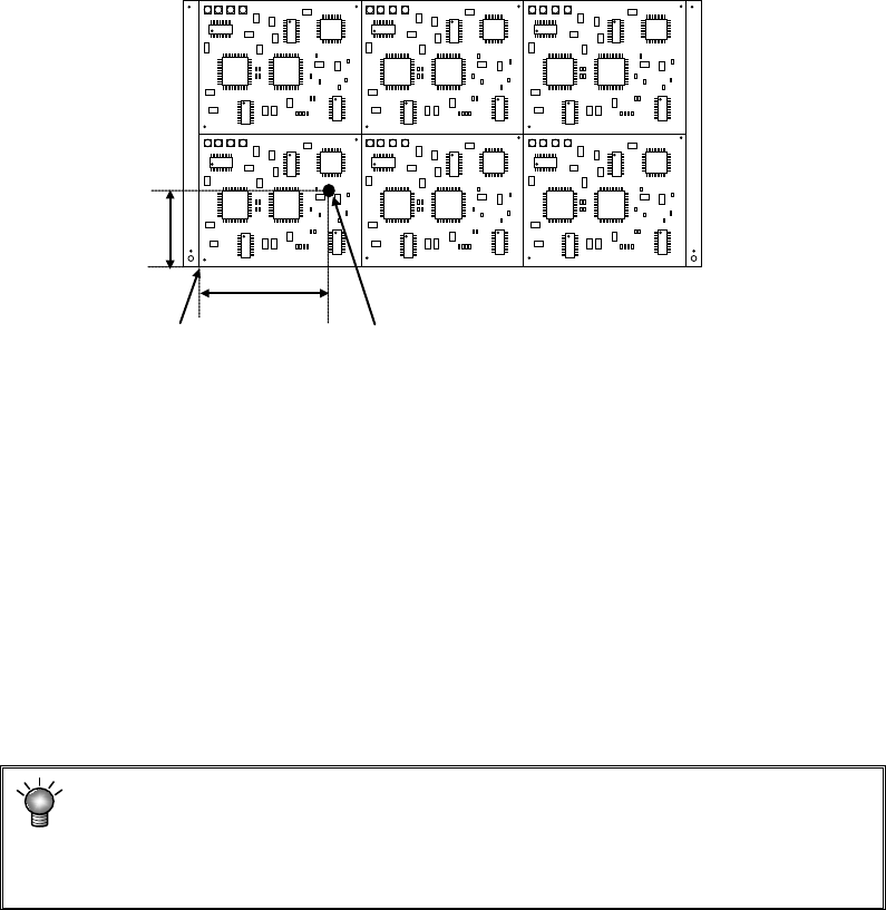
Example: Data entry for a multi-plane matrix PWB
The following examples indicate a PWB whose reference circuit is at the left bottom
corner, and whose circuit origin is at the left bottom corner of a circuit.]
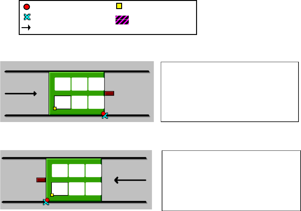
① For front reference and PWB transport direction of L → R: (when “Shape reference” is
selected as the “Positioning method” on the “Basic setting” screen)
② For front reference and PWB transport direction of R → L: (when “Shape reference” is
selected as the “Positioning method” on the “Basic setting” screen)
PWB dimensions X=200 Y=120
PWB layout offset X=5 Y=−5
Circuit dimension X=50 Y=30
Ckt. Layout offset X=0 Y=0
First circuit position X=−170 Y=15
Circuit divide No X=3 Y=2
Circuit pitch X=60 Y=50
PWB dimensions X=200 Y=120
PWB layout offset X=−5 Y=−5
Circuit dimension X=50 Y=30
Ckt. Layout offset X=0 Y=0
First circuit position X=20 Y=15
Circuit divide No X=3 Y=2
Circuit pitch X=60 Y=50
:PWB position reference
:
Transport direction
:Circuit origin
:Reference circuit
:Layout end