JX-350_EPU使用说明书.pdf - 第84页
EPU Instruction M anual C hapter 4 Creating a Production Progr am 4- 36 ♦ Mu lt i - circ uit ma trix The order of circuits is the X - direction pitch/Y - direct ion pitch fr om the ref eren ce circuit . ♦ Mu lt i - circu…
EPU Instruction Manual Chapter 4 Creating a Production Program
4-35
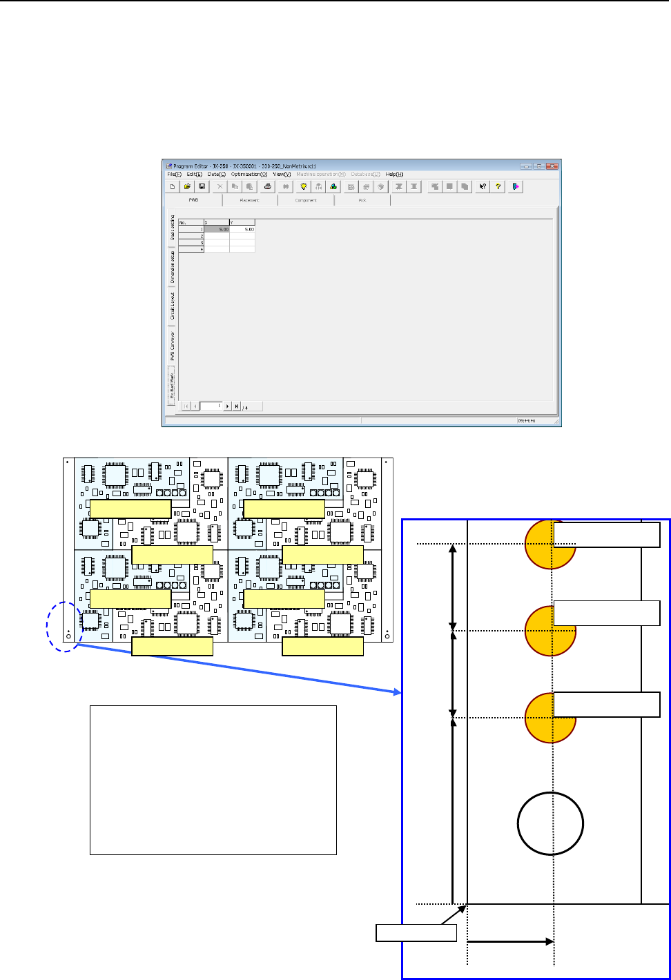
4.1.2.5 “Ex. Bad Mark” screen
For the extended bad mark, enter the "bad mark" position for each circuit from the "PWB
reference position."
Use this mark when the head moving distance for recognition is shortened or a mark
cannot be created in the circuit.
When you use an extended bad mark, enter the coordinates of a bad mark on each circuit.
When you select the “Ex. Bad Mark” tab displayed on the lower left of each “PWB” data
screen, the following screen appears.
Circuit No.1 X=5 Y=10
Circuit No.2 X=5 Y=17
Circuit No.3 X=5 Y=24
Circuit No.4 X=5 Y=31
Circuit No.5 X=5 Y=38
Circuit No.6 X=5 Y=45
Circuit No.7 X=5 Y=52
Circuit No.8 X=5 Y=59
For circuit No.1
For circuit No.2
For circuit No.3
5mm
10mm
7mm
7mm
PWB origin
Circuit No.1
Circuit No.3
Circuit No.4
Circuit No.2
Circuit No.5
Circuit No.6
Circuit No.7
Circuit No.8
EPU Instruction Manual Chapter 4 Creating a Production Program
4-36
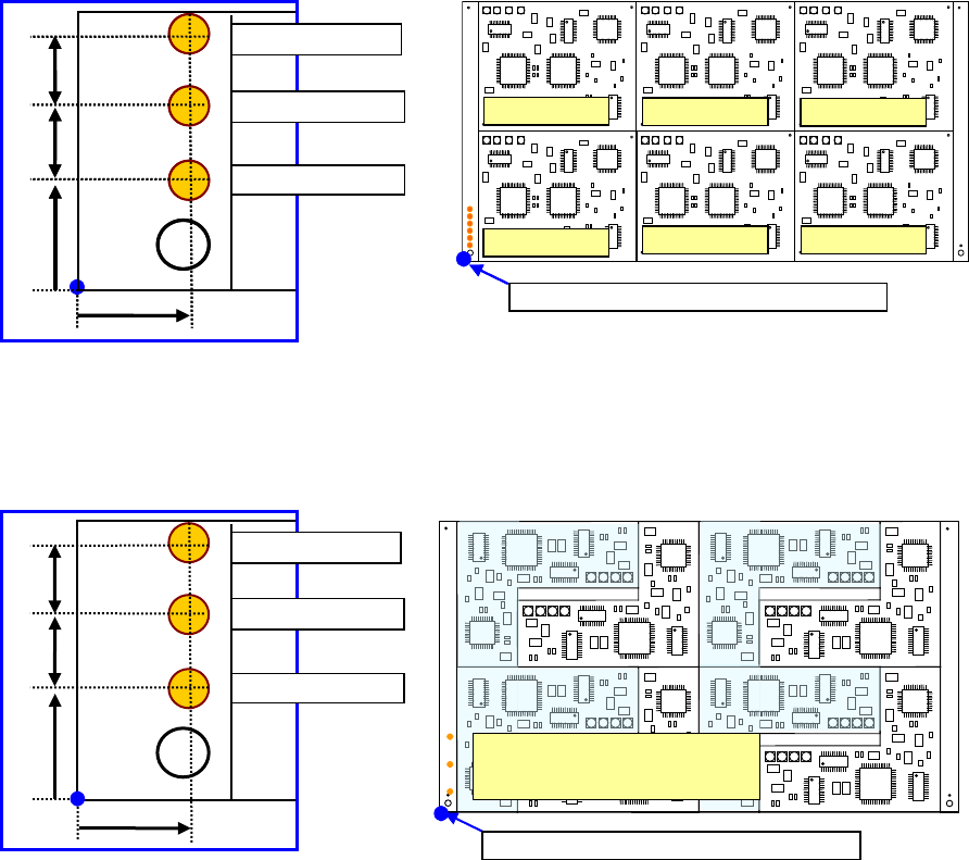
♦ Multi-circuit matrix
The order of circuits is the X-direction pitch/Y-direction pitch from the reference
circuit.
♦ Multi-circuit non-matrix
The order of circuits set by circuit arrangement is used.
For circuit No.1
For circuit No.3
10mm
7mm
For circuit No.2
5mm
7mm
PWB position reference [PWB origin]
Circuit No.4
PWB position reference [PWB origin]
Circuit No.1
Circuit No.2
Circuit No.3
Circuit No.5
Circuit No.6
For circuit No.1
For circuit No.3
10mm
7mm
For circuit No.2
5mm
7mm
The order may depend on
the circuit layout No.
For circuit No.1
For circuit No.3
10mm
7mm
For circuit No.2
7mm
5mm
PWB position reference [PWB origin]
EPU Instruction Manual Chapter 4 Creating a Production Program
4-37
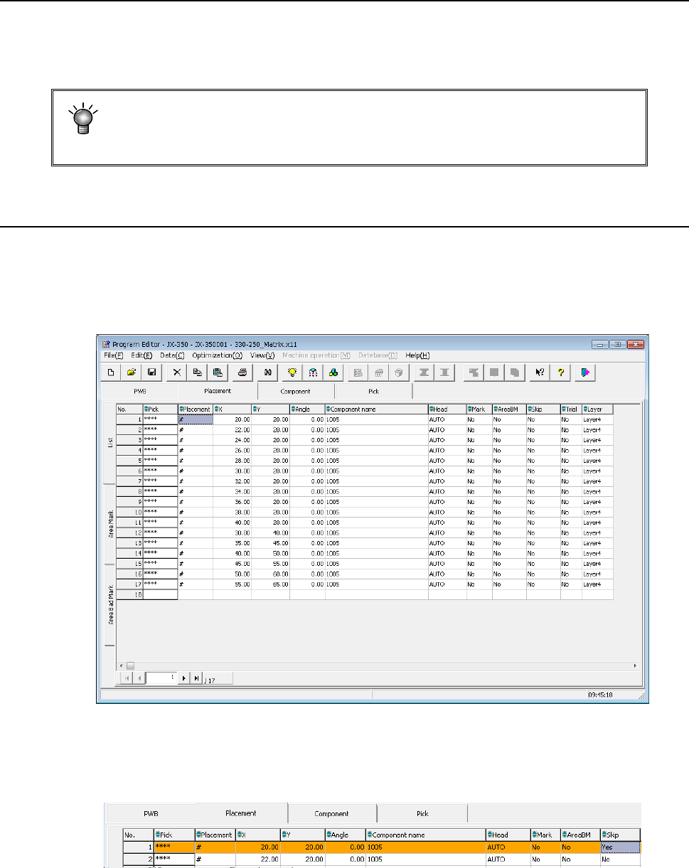
4.1.3 Placement data
Enter information on the coordinates of positions on which the system is to place
components.
For a multi-plane PWB, enter the information on the “reference circuit.”
Number of component placements:
You can enter total of 10,000 placements regardless of the PWB type,
normal or divided type.
4.1.3.1 Viewing the placement data screen
When you click the “Placement” tab displayed on the screen after creating PWB data
completely, the “Placement” data screen for creating Placement data (the following figure
is an example indicating that Placement data was already created) appears on the
screen.
When any skip setting (including component data skip setting) is performed, the indication
is changed into orange as shown below.