JX-350_EPU使用说明书.pdf - 第93页
EPU Instruction M anual C hapter 4 Creating a Production Progr am 4- 45 “ Displayed menu items ” • Ma r k I D: Enter a mark ID. Y ou can enter up t o eight half - charac ters. W hen you omit it , the system aut omaticall…
EPU Instruction Manual Chapter 4 Creating a Production Program
4-44
3) Creating Mark data
Select the “Area Bad Mark” tab to open the “Area Bad Mark” edit screen.
When you press the <F9> key on the “Placement” data list screen or select the
“Edit” or “Browse” menu item on the pop-up menu, you can open this screen also.
If you double-click the “Area Bad Mark” tab when the focus is in the “AreaBM”
field of the “Placement” data list screen, the “Area Bad Mark” screen opens in
Read Only mode.
The area bad marks already registered appear in the area bad mark list.
Select an area bad mark to be used among them.
To register a mark anew, move the focus to a line in which no data is entered yet and
enter the X-coordinate and Y-coordinate of the mark.
The area bad mark editing screen can be opened by the following method. The
contents of processing depend on each display mode
Operation Screen mode
"Edit" is selected in the area bad mark pop-up menu. Editing/selection mode
"View" is selected in the area bad mark pop-up menu Selection mode
The area bad mark tab is clicked. Editing mode
The cell is double-clicked at mark. Selection mode
Screen mode Contents of processing
Selection mode The area bad mark data to be used by the placement data is
registered. The cursor on the list is displayed in a line
selection status. The "OK" button is indicated in light color.
Editing mode The coordinates of the area bad mark can be entered and
registered. The "Select" button is not displayed.
Editing/selection mode Selection and editing can be performed simultaneously.
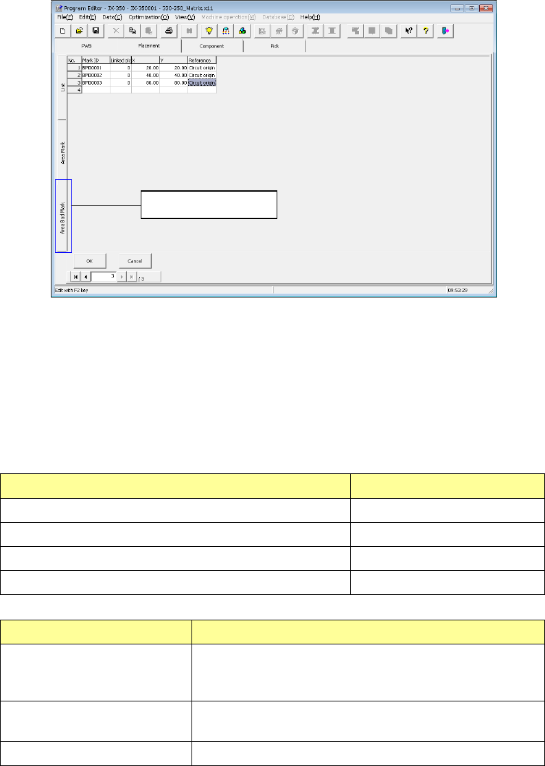
Area Bad Mark tab

EPU Instruction Manual Chapter 4 Creating a Production Program
4-45
“Displayed menu items”
• Mark ID: Enter a mark ID. You can enter up to eight half-characters.
When you omit it, the system automatically assigns an ID to the
mark.
• Linked pla: Displays the number of placement data records that refer to the area
bad marks when you open the “Area Bad Mark” screen. You cannot
edit this item.
• X: Enter the X dimension from the position regulated in the “Reference”
field to the center of the area mad mark.
• Y: Enter the Y dimension from the position regulated in the “Reference”
field to the center of the area mad mark.
• Reference: Select the reference position of the coordinate system, the origin of
the circuit (circuit reference position) or that of the board (board
reference position).
If selection is performed from the pop-up menu when the cursor is at "Reference" and
multiple lines are selected, the same value is set for all the selected records.
Note: For a single-circuit PWB, the circuit reference can be selected. In this case,
set the coordinates from the home position of the PWB. The coordinate values for X
and Y can be obtained by teaching.
Each of the above items cannot be edited when the screen is opened by "View."
When the screen is opened by "View", they are displayed in the line selection mode.
“Operation buttons”
• OK: Saves the edited data and returns to the “Placement” data list screen.
At that time, the use of mark group is not set.
• Cancel: Discards your editing and returns to the “Placement” data list screen.
When you double-click or press the Placement list tab to quit this “Area Bad Mark”
screen, the system redisplays the “Placement” data list screen without setting any link
to the Placement data.
The color of a bad mark should be able to be distinguished from that of a board, and
its diameter should be 2.5 mm or more. Note that when you use a bad mark, the
cycle time becomes longer by the mark recognition time.
(9) Skip
When you select “Yes” for this field, the system skips component placement on the
corresponding position: that is, the system does not place any component on the
position specified on this line. This function is mainly used for checking.
As the initial value, "No" is set.
To make a change, press the Edit key or right-button of the mouse and select data
from the list.
If data is selected from the pop-up menu when the cursor is at "Skip" and multiple
lines are selected, the same value is set for the all the selected records.
EPU Instruction Manual Chapter 4 Creating a Production Program
4-46
(10) Trial
Set the test run to "Yes" or "No." When the specified placement point is specified in
the test run range of the production condition screen, a test run is executed for only
the placement data which is specified to "Yes" in this item.
As the initial value, "No" is set.
To make a change, press the Edit key or right-button of the mouse and select data
from the list.
If data is selected from the pop-up menu when the cursor is at "Skip" and multiple
lines are selected, the same value is set for the all the selected records.
(11) Layer
This function allows you to specify the order of component placement.
The lower numbers will be given the higher priority (i.e., to be placed earlier). As the
initial value, "4" is set.
When optimization is executed, the order of placement will be automatically defined
regardless of the data input order. (When “No components” occurs at production, it is
impossible to proceed to the production of the next layer unless the production of a
younger No. layer is completed.) Then, the system refers to the layers to determine
the optimized component placement order on the same layer.
To make a change, press the Edit key or right-button of the mouse and select data
from the list.
If selection is performed from the pop-up menu when the cursor is at "Reference" and
multiple lines are selected, the same value is set for all the selected records.
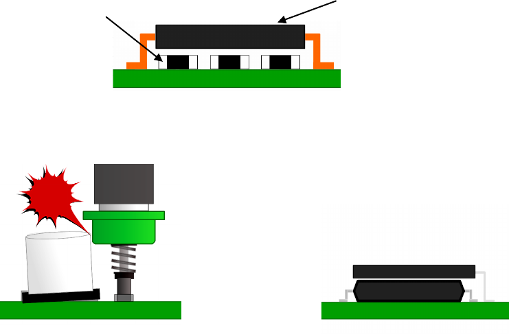
Example) If the system places QFP components and a chip component as shown in the
figure below, it has to place a chip component first.
In this example, when you specify the layer 4 for a chip component, and the
layer 5 for a QFP, the system places a chip component whose layer number is
smaller first, and then a QFP.
<Placing QFP on the chip.>
・Layers are also used for adjacent placement/laminated placement.
<A component is placed near a tall one.>
<IC components are stacked.>
Chip component (layer 4)
QFP (layer 5)