JX-350_EPU使用说明书.pdf - 第74页
EPU Instruction M anual C hapter 4 Creating a Production Progr am 4- 26 10) B ad mark position: It is selected whether t he bad mark is used or not. W hen you select “ No - use ” , “ *** ” is displayed. W hen you select …
EPU Instruction Manual Chapter 4 Creating a Production Program
4-25
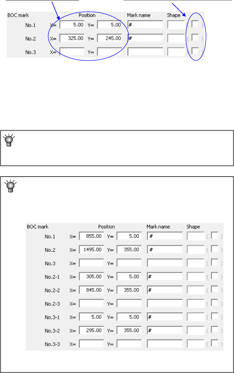
9) BOC mark position, Mark name, Shape:
Enter the distance from the PWB origin or the circuit origin to the center of a BOC
mark.
Enter the “Mark name” and “Shape” fields in the same manner as a single-plane
PWB (“Single PWB” as the “PWB configuration”).
♦ Using 2 points: It is possible to correct the difference between the design dimensions
and the actual dimensions (measured dimensions) and the rotation direction error.
For the third point, leave the field blank.
When there are multiple marks on the PWB, select 2 points on the diagonal lines in
all the placement range.
♦ For using 3 points: In addition to the case of two points, the perpendicularity distortion
between the X axis and Y axis can be corrected.
When “PWB marks are used” is selected as “BOC type” on the “Basic
setting” screen, this is the distance from the PWB origin to a BOC mark.
When “Circuit marks are used” is selected, this is the distance from the
circuit origin to a BOC mark.
For using a long PWB:
For a large-shaped PWB whose external length X exceeds 650mm, set
the first and second BOC marks; for an optional large-shaped PWB whose
external length X exceeds 1200mm, set the first, second and third BOC
marks.
However, if the circuit is divided in the X direction and circuit BOC exists,
an error may be displayed at the start of production, disabling production.
JX-350 EPU is not applicable to the teaching.
Enter the X and Y coordinates.
EPU Instruction Manual Chapter 4 Creating a Production Program
4-26
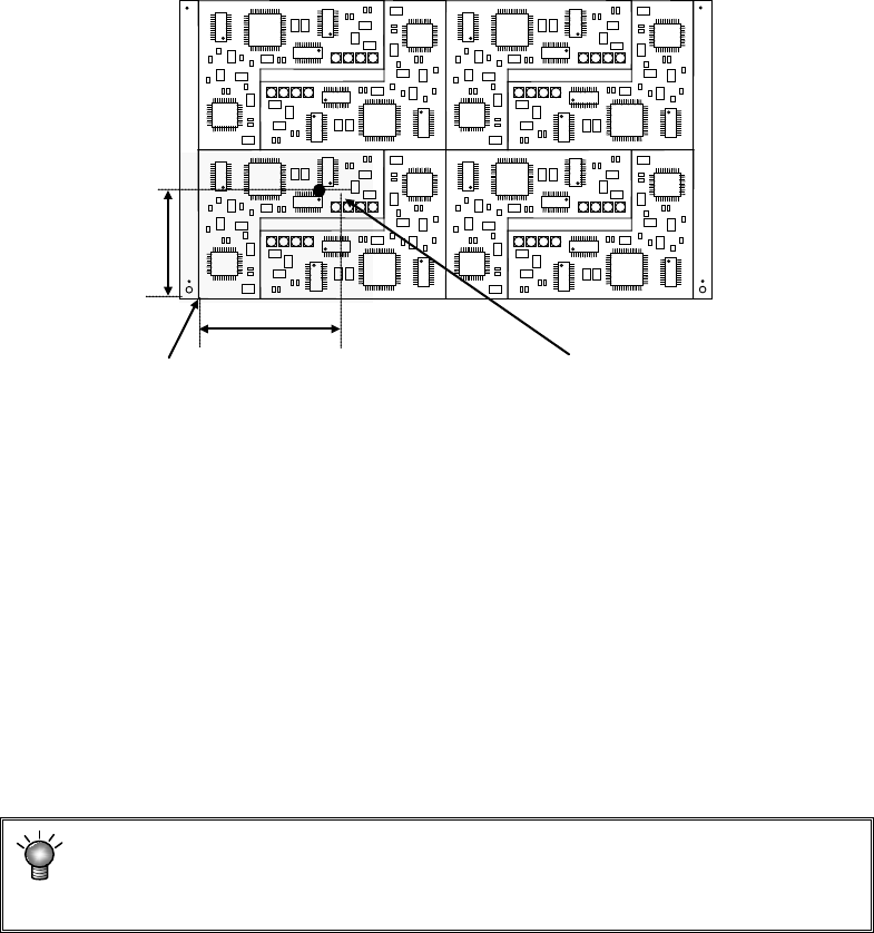
10) Bad mark position:
It is selected whether the bad mark is used or not. When you select “No-use”,
“***” is displayed. When you select “Use”, enter the length from the circuit origin
(circuit position reference) to the bad mark center position.
* In the above case, enter X = a and Y = b.
<Usage of a bad mark and the operation flow>
i) Enter coordinates of a bad mark into PWB data (that is, to the “Bad mark
position” fields.)
ii) At machine setup, adjust the bad mark reader.
iii) Before feeding a PWB, affix a bad mark at the spot specified with the bad
mark coordinates on a defective circuit.
iv) Before the start of production, the OCC or bad mark sensor reads a bad mark of
each circuit. When a bad mark is recognized, components are not placed on the
corresponding circuit.
The requirements for a bad mark: the mark must be distinct in the color
from a PWB, and its diameter must be 2.5 mm or greater. If a bad mark
is used, the production time will be longer by the mark recognition time.
* For the extended bad mark, see "4.1.2.5 "Ex. bad mark" screen."
* If the bad mark is set out of the circuit, use an extension bad mark.
11) PWB height, PWB thickness, and Back height:
Enter these fields in the same manner as those for a single-plane PWB.
a
b
Circuit origin (circuit position reference)
Coordinates of a bad mark
EPU Instruction Manual Chapter 4 Creating a Production Program
4-27
4.1.2.3 Circuit Layout
Specify the circuit position and angle, and circuits to be placed on a board. Only when you
select the “Used” radio button for the menu item “Circuit Mapping” on the “Basic setting” tab,
and the “Matrix circuit” radio button or the “Non-matrix circuit” radio button in the “PWB
configuration” column of the “Dimension setup” tab, you can select these items. When you
select the “Not Used” radio button for the menu item “Circuit Mapping” on the “Basic setting” tab,
you can select these items only if you select the “Non-matrix circuit” radio button.
When you select the “Circuit Layout” tab located on the lower left corner of the “Dimension
setup” screen, the following screen appears.
1) Circuit position (X,Y)
In case of a matrix-circuit board, the system calculates the X and Y coordinates based
on the board settings entered on the “Dimension setup” tab to display them. In case of
a non-matrix circuit board, enter the distance from the board reference position to the
origin of each circuit and the angle.
Enter the dimensions from the board reference position to the home position of each
circuit in the “X” and “Y” fields respectively.
2) Angle
In case of a multi-circuit board, “0” is displayed in the “Angle” field. In case of a
non-matrix board, enter the assignment angle of each circuit.
In the “Angle” field, enter a value on the assumption that the angle used when you enter
values in the “Circuit dimensions” fields and the “Circuit layout offset” fields on the
“Dimension setup” screen is regarded as 0 degrees, and the anti-clock direction as “+.”
(When you use CAD data for the component placement coordinates, the angle of the
circuit that matches the CAD data is regarded as 0 degrees.)