IPC-TM-650 EN 2022 试验方法--.pdf - 第105页
Figure 3 Pattern of One T est Board Showing Three T est Substructures (Board is 150 mm sq.) IPC-TM-650 Number Subject Date Revision Page 2 of 4 2.2.21 Planarity of Dielectrics for High Density Interconnection (HDI)/ Micr…
IPC-DD-135
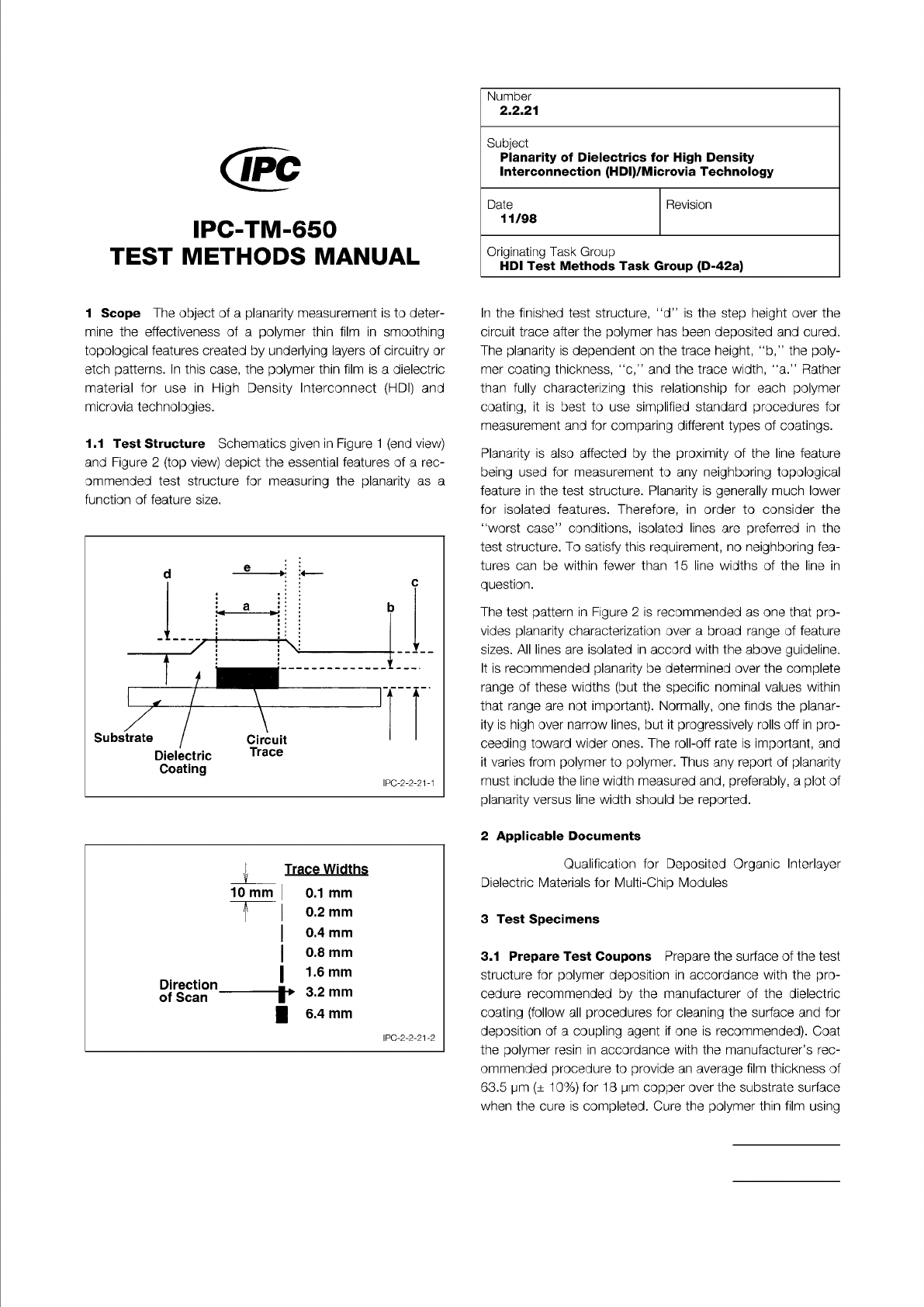
Figure 1 Cross-Section Planarization Diagram
Figure 2 Top View of Planarization Structure
The Institute for Interconnecting and Packaging Electronic Circuits
2215 Sanders Road • Northbrook, IL 60062
Material in this Test Methods Manual was voluntarily established by Technical Committees of the IPC. This material is advisory only
and its use or adaptation is entirely voluntary. IPC disclaims all liability of any kind as to the use, application, or adaptation of this
material. Users are also wholly responsible for protecting themselves against all claims or liabilities for patent infringement.
Equipment referenced is for the convenience of the user and does not imply endorsement by the IPC.
Page 1 of 4
IPC-TM-650
TEST
METHODS
MANUAL
1
Scope
The
object
of
a
planarity
measurement
is
to
deter¬
mine
the
effectiveness
of
a
polymer
thin
film
in
smoothing
topological
features
created
by
underlying
layers
of
circuitry
or
etch
patterns.
In
this
case,
the
polymer
thin
film
is
a
dielectric
material
for
use
in
High
Density
Interconnect
(HDI)
and
microvia
technologies.
1.1
Test
Structure
Schematics
given
in
Figure
1
(end
view)
and
Figure
2
(top
view)
depict
the
essential
features
of
a
rec¬
ommended
test
structure
for
measuring
the
planarity
as
a
function
of
feature
size.
]
Trace
Widths
10
mm
|
0.1
mm
,
0.2
mm
0.4
mm
Direction
of
Scan
0.8
mm
1.6
mm
3.2
mm
.
6.4
mm
I
PC-2-2-21
-2
Number
2.2.21
Subject
Planarity
of
Dielectrics
for
High
Density
Interconnection
(HDI)/Microvia
Technology
Date
Revision
11/98
Originating
Task
Group
HDI
Test
Methods
Task
Group
(D-42a)
In
the
finished
test
structure,
''d"
is
the
step
height
over
the
circuit
trace
after
the
polymer
has
been
deposited
and
cured.
The
planarity
is
dependent
on
the
trace
height,
"b/'
the
poly¬
mer
coating
thickness,
llc,"
and
the
trace
width,
"a.”
Rather
than
fully
characterizing
this
relationship
for
each
polymer
coating,
it
is
best
to
use
simplified
standard
procedures
for
measurement
and
for
comparing
different
types
of
coatings.
Planarity
is
also
affected
by
the
proximity
of
the
line
feature
being
used
for
measurement
to
any
neighboring
topological
feature
in
the
test
structure.
Planarity
is
generally
much
lower
for
isolated
features.
Therefore,
in
order
to
consider
the
"worst
case"
conditions,
isolated
lines
are
preferred
in
the
test
structure.
To
satisfy
this
requirement,
no
neighboring
fea¬
tures
can
be
within
fewer
than
15
line
widths
of
the
line
in
question.
The
test
pattern
in
Figure
2
is
recommended
as
one
that
pro¬
vides
planarity
characterization
over
a
broad
range
of
feature
sizes.
All
lines
are
isolated
in
accord
with
the
above
guideline.
It
is
recommended
planarity
be
determined
over
the
complete
range
of
these
widths
(but
the
specific
nominal
values
within
that
range
are
not
important).
Normally,
one
finds
the
planar¬
ity
is
high
over
narrow
lines,
but
it
progressively
rolls
off
in
pro¬
ceeding
toward
wider
ones.
The
roll-off
rate
is
important,
and
it
varies
from
polymer
to
polymer.
Thus
any
report
of
planarity
must
include
the
line
width
measured
and,
preferably,
a
plot
of
planarity
versus
line
width
should
be
reported.
2
Applicable
Documents
Qualification
for
Deposited
Organic
Interlayer
Dielectric
Materials
for
Multi-Chip
Modules
3
Test
Specimens
3.1
Prepare
Test
Coupons
Prepare
the
surface
of
the
test
structure
for
polymer
deposition
in
accordance
with
the
pro¬
cedure
recommended
by
the
manufacturer
of
the
dielectric
coating
(follow
all
procedures
for
cleaning
the
surface
and
for
deposition
of
a
coupling
agent
if
one
is
recommended).
Coat
the
polymer
resin
in
accordance
with
the
manufacturer's
rec¬
ommended
procedure
to
provide
an
average
film
thickness
of
63.5
pm
(±
1
0%)
for
1
8
pm
copper
over
the
substrate
surface
when
the
cure
is
completed.
Cure
the
polymer
thin
film
using
Figure 3 Pattern of One Test Board Showing Three Test Substructures (Board is 150 mm sq.)
IPC-TM-650
Number
Subject Date
Revision
Page 2 of 4
2.2.21
Planarity
of
Dielectrics
for
High
Density
Interconnection
(HDI)/
Microvia
Technology
11/98
all
steps
recommended
for
full
curing.
For
resin
coated
cop¬
per
(RCC)
foil,
after
laminating
the
foil,
cure
as
per
manufac¬
turer's
instructions,
then
etch
the
copper
layer
and
proceed
as
for
other
deposited
dielectric
materials
(see
Figure
3).
4
Equipment/Apparatus
This
method
uses
profilometer
measurements
providing
topological
height
variations
as
a
function
of
displacement
across
the
surface
of
a
standard
test
structure.
Use
a
TENCOR
Profilometer
(Model:
Alpha
Step
200).
Substi¬
tutions
are
acceptable,
provided
they
can
measure
feature
heights
in
the
range
used
to
within
土
2%
and
can
provide
a
linear
scan
of
at
least
10
mm.
Note:
As
an
alternate
method,
where
a
profilometer
is
not
available,
the
measurements
can
be
collected
by
cross¬
sectioning
the
test
structures.
This
method
will
require
one
cross-section
for
each
trace
width
in
order
to
collect
data
for
trace
width
effects.
5
Procedure
Prior
to
the
polymer
deposition,
scan
the
pro¬
filometer
stylus
across
all
copper
lines
in
the
test
structure,
scanning
in
the
direction
indicated
by
the
arrow
in
Figure
2.
Measure
and
record
the
dimensions
depicted
as
“a”
and
"b”
in
Figure
1
for
each
of
the
lines.
After
polymer
deposition
and
cure,
measure
the
polymer
film
thickness
at
a
location
distant
(at
least
1
5
line
widths)
from
any
of
the
test
structure's
copper
lines.
In
order
to
do
this,
a
''win-
dow!,
must
be
imaged
in
the
dielectric
down
to
the
substrate.
A
,(window"
to
the
substrate
may
be
opened
by
photo¬
imaging,
chemical
dissolution,
laser
ablation,
or
other
appro¬
priate
method
(see
Figure
4).
The
sweep
must
allow
measure¬
ments
of
the
thickness
of
the
dielectric
entering
and
exiting
the
''window.”
These
measurements
should
be
within
±
0.2
pm
of
each
other.
Record
this
dielectric
thickness
as
dimen-
sion
"c."
Finally,
measure
the
dimension
shown
in
Figure
1
as
the
fea¬
ture
step
height
"cT
of
the
polymer;
use
the
profilometer,
not
an
optical
method.
In
measuring
"dj
take
the
difference
in
height
between
the
highest
point
on
top
of
the
copper
line
and
the
lowest
point
at
least
15
line
widths
from
the
line
to
be
measured.
5.1
Conditions
of
Test
5.1.1
Calibrate
the
profilometer
before
making
measure¬
ments
using
the
calibration
procedure
specified
by
the
manu¬
facturer
of
the
equipment.
5.1.2
Measure
at
ambient
room
temperature
and
humidity.
I
PC-2-2-21
-3
IPC-TM-650
Number
Subject Date
Revision
Page 2 of 2
4/73
2.3.1
Chemical
Processing,
Suitable
Processing
Material
5.3.4
Drill
1.5
mm
holes
in
the
pads
of
the
3
mm
lines
with
good
fabricating
practice.
5.3.5
Remove
the
developed
KPR
by
rubbing
the
pattern
lightly
with
cold
trichlorethylene
liquid.
Rinse
in
water.
Scrub
the
specimens
with
FFF
pumice
and
water
with
a
strong
bristle
brush.
5.3.6
Plate
(this
is
simulated
plating)
per
MIL-P-1
3949.
5.3.7
Deoxidize
by
dipping
in
10%
hydrochloric
acid
for
two
minutes
and
wash
in
running
water
for
five
minutes.
Dry
30
minutes,
minimum,
at
105℃
to1
10℃.
5.3.8
Coat
the
etched
copper
surface
with
white
petrola¬
tum.
Specimens
shall
be
immersed
horizontally
in
solder
6.5
mm
below
the
surface
for
20
土
1
seconds
at
260℃
+5/-0℃
measured
25
mm
below
the
surface.
5.3.9
Remove
the
petrolatum
from
the
surface
of
the
speci¬
men
with
a
two
minute
scrub
in
cold
trichlorethylene,
followed
by
a
one
minute
rinse
in
hot
trichlorethylene.
5.3.10
Inspect
the
surface
for
weave
exposure,
measling,
crazing,
resin
loss,
delamination,
and
blistering.
5.3.11
Test
four
1
mm
lines
on
the
specimen
for
peel
strength
per
MIL-P-13949,
reporting
the
average
value
for
the
four
lines.