IPC-TM-650 EN 2022 试验方法--.pdf - 第644页
Example: R n = R 0 = 50 Ω , I 0 = 14 mA, I s = 6 mA. At n = 1 1 step I 11 = 80 mA and the corresponding applied power P 11 = (0.014 A + 11 * 0.006 A) 2 * 50 Ω = 0.32 W. 5.3.3 Linear Power S teps Setting the voltage or cu…
plating, circuit developing baths and soldering re-flows. Mate-
rials so affected should be brought to equilibrium with appro-
priate atmosphere and temperature control before testing.
Description of the conditioning should be included in the test-
ing report.
5 Apparatus
The method requires a power source meter
and electrical resistance meter, such as Keithley
1
Source
Meter or equivalent, for sourcing the applied DC power and
measuring the resulting current resistance. The resolution
of resistance measurements should be in the range of about
0.1 Ω or better.
5.1 Power requirements
The power capacity of the
power sourcing instrumentation should be sufficient to main-
tain the test power until it reaches the value defined in the test
failure/acceptance criteria where the specimen-maximum
power will be dissipated. The voltage level should be stable to
within ± 0.1% of the set value during the testing time. An out-
put current of 1 µA to 1 A is usually sufficient for most testing
conditions. The power dissipated during the test may vary
depending on the specimen resistance thermal characteris-
tics, and the failure mechanism.
5.2 Circuit controls
The apparatus should be equipped
with a circuit breaking device with adjustable current/voltage
sensors, and be capable of disconnecting the power source
in the case of overloading conditions. The current/voltage-
sensing circuit should measure the specimen power and allow
for adjustment consistent with the specimen characteristics.
The sensing device should respond at the power level that is
indicative of the test conditions reaching the failure criteria.
5.3 Power level controls
The power level should be
adjustable with the possibility of setting discrete power level
values in at least 20 steps. It is recommended that the initial
power P
0
is set at 1/10 of the nominal operational power of
the device. A computerized experimental set-up is recom-
mended to carry out the test.
In the case of sourcing voltage, the initial voltage, V
0
=
√
0.1
*
P
nom
*
R
0
. For example, if the initial value of R
0
= 50
Ω and P
nom
= 0.1 W then the initial voltage V
0
corresponding
to 0.1 of P
nom
(i.e., P
0
= 0.010 W), is
√
0.1
*
0.1 W
*
50 Ω ≈
0.7 V. The voltage level V
n
should be increased in steps of V
s
≤ V
0
, each step having duration of about 60 s. The specimen
current I
n
should be monitored and recorded at every power
step (see 5.3.1).
In the case of sourcing current, the initial current, I
0
=
√
0.1
*
P
nom
/ R
0
. For example, if the initial value of R
0
= 50
Ω and P
nom
= 0.1 W, then the initial voltage V
0
corresponding
to 0.1 of P
nom
(i.e., P
0
= 0.010 W), is
√
0.1
*
0.1 W / 50 Ω ≈
0.014 A. The current level I
n
should be increased in steps of I
s
≤ I
0
, each step having a duration of about 60 s. The specimen
voltage V
n
should be monitored and recorded at every power
step (see 5.3.2).
5.3.1 Linear Voltage Steps
Increasing voltage in constant
voltage steps will result in a quadratic increase of power. At
the n
th
voltage step the power P
n
is given by (5):
P
n
= (V
0
+ nV
s
)
2
/ R
n
(5)
Example: R
n
= R
0
= 50 Ω, V
0
= 0.7 V, V
s
= 0.3 V. At n = 11
step V
11
= 4 V and the corresponding applied power P
11
=
(0.7 V + 11
*
0.3V)
2
/ 50 Ω = 0.32 W.
5.3.2 Linear Current Steps
Increasing current from I
0
by
adding a constant current step, I
s
, will result in a quadratic
increase of applied power. At the n
th
current step the power
P
n
is given by (6):
P
n
= (I
0
+ nI
s
)
2
*
R
n
(6)
1. Certain commercial equipment and materials are identified in this document in order to specify adequately the experimental procedure. In no case does such
identification imply recommendations nor does it imply that the material or equipment identified is necessarily the best available for this purpose.
Number
2.5.34
Subject
Power Density Rating for Embedded Resistors
Date
07/12
Revision
IPC-TM-650
o
o
o
o
o
o
o
o
o
o
o
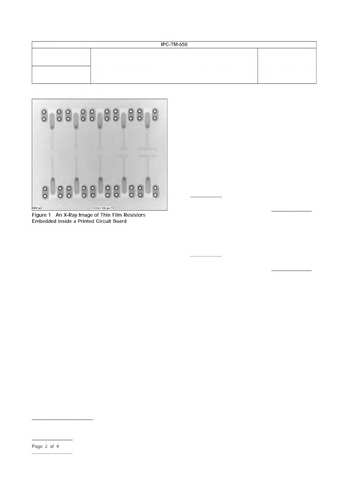
Figure
1
An
X-Ray
Image
of
Thin
Film
Resistors
Embedded
Inside
a
Printed
Circuit
Board
Page
2
of
4
Example: R
n
= R
0
= 50 Ω, I
0
= 14 mA, I
s
= 6 mA. At n = 11
step I
11
= 80 mA and the corresponding applied power P
11
=
(0.014 A + 11
*
0.006 A)
2
*
50 Ω = 0.32 W.
5.3.3 Linear Power Steps
Setting the voltage or current
stimulus for linear increase in the applied power is given by (7)
and (8) respectively:
V
n
=
√
(P
0
+ nP
s
)
*
R
n
(7)
I
n
=
√
(P
0
+ nP
s
) / R
n
(8)
Example: R
n
= R
0
= 50 Ω, P
0
= 0.01 W, P
s
= 0.01 W. At step
n = 11 the applied power P
11
= 0.01 + 11
*
0.01 = 0.12 W.
The corresponding voltage stimulus V
11
=
√
0.12 W
*
50 Ω ≈
2.5 V. In the case of sourcing current the corresponding cur-
rent stimulus I
11
=
√
0.12 W / 50 Ω ≈ 0.048 A.
6 Procedure
Testing should be performed at ambient con-
ditions; temperature (t
0
) = 22 °C ± 3 °C [71.6 °F ± 5.4 °F] and
relative humidity (RH
0
) = 50% ± 10% (see IPC-TM-650,
Method 1.3, Ambient Conditions).
6.1
Measure the initial stable resistance, R
0
at the ambient
temperature (t
0
) and relative humidity (RH
0
).
6.2
Apply a constant power step P
n
for a period of 60 s,
until temperature stabilizes and a steady current reading is
reached (see 5.3).
6.3
Record voltage V
n
and the resulting current I
n
. Calculate
the actual P
n
from equation (2).
6.4
Disconnect the power for a period of time sufficient for
the device to return to the ambient temperature conditions t
0
.
Measure the device resistance R
n
. Calculate the relative differ-
ence between the measured resistance and the nominal resis-
tance:
(∆R)
r
= (R
n
− R
0
) / R
0
(9)
6.5
Continue stepping up the applied power (6.2 - 6.4) for
P
max
and/or P
failure
until the relative change in resistance, (∆R)
r
= (R
n
- R
0
) / R
0
approaches a value indicative of failure or
acceptance criteria.
6.6
After recording P
max
, calculate PDR using equation (4).
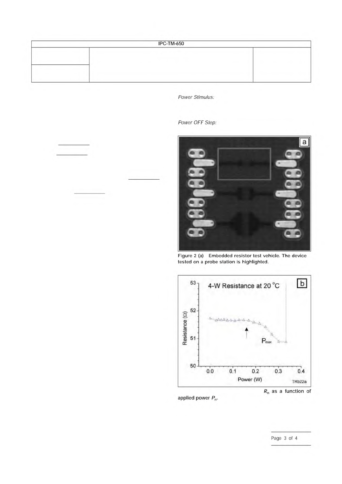
7 Test Example
An embedded resistor R
0
= 50 Ω, S =
0.77 mm
*
0.58 mm ≈ 0.44 mm
2
, shown in Figure 2a was
tested under the following conditions:
Linear voltage steps (5.3.1), P
0
= 0.01 W, V
0
= 0.7 V, V
s
= 0.2 V, power step ON = 60 s.
Recording: current I
n
, voltage V
n
, power P
n
.
20 s (typical). Recording 4-W resistance R
n
.
Figure 2b illustrates the test results. The stable resistance
value R
0
is about 51.7 Ω. It remains stable until the power
Figure 2 (b) Recorded resistance
Number
2.5.34
Subject
Power Density Rating for Embedded Resistors
Date
07/12
Revision
IPC-TM-650
—
Power
Stimulus:
Power
OFF
Step:
Figure
2
(a)
Embedded
resistor
test
vehicle.
The
device
tested
on
a
probe
station
is
highlighted.
4-W
Resistance
at
20
°C
国
50
-
•
I
J
1
*
1
I
1
r
•
i
1
1
'
*
I
•
'
•
-
k
0.0
0.1
0.2
0.3
0,4
Power
(W)
trm;
applied
power
Pn.
Rn
as
a
function
of
Page
3
of
4

level approaches 0.160 W. With increasing power above
0.160 W the resistance value gradually starts to deviate from
its stable value. The resistor fails ‘‘open’’ at P
failure
of 0.360 W.
The resistance plot in Figure 2b suggests that P
max
≈0.160 W.
Thus in the above illustration, the power density rating for that
resistor, for which S ≈ 0.44 mm
2
, calculated from equation (4),
PDR = 0.16 W / 0.44 mm
2
≈ 0.36 W / mm
2
.
7.1 PDR Safety Factor
In the example above, the surface
temperature at the tested resistors measured (optionally) at P
n
= 0.160 W was about 42 °C. Depending on the material’s
physical characteristics, this heating effect might lead to an
accelerating aging and shortening the device operational life.
Therefore it is recommended that P
max
is reduced accordingly
by a certain safety factor that can be deduced, for example,
from the aging study.
8 Accuracy Considerations
Several uncertainty factors
such as instrumentation, dimensional uncertainty of the test
specimen geometry, resistance of contacts and interconnects
among others contribute to the combined uncertainty of the
measurements. The complexity of modeling these factors may
be considerably higher when the measurements are per-
formed at elevated temperatures for resistors embedded in
complex multilayer assemblies. Adequate analysis can be per-
formed, however, using the partial derivative technique for
equation (4) It is recommended that the combined instrumen-
tation uncertainties should be 10 times smaller than the nomi-
nal tolerance value of the resistor. Likewise, it is recom-
mended that uncertainty in the surface area, S, is considered
very carefully since S is the primary parameter used in scaling
the PDR ratings for different form-factor resistors.
Additional limitations may arise from the systematic uncer-
tainty of the particular instrumentation, calibration standards,
and the dimensional imperfections of the actually imple-
mented test specimen. The test may require specialized
instrumentation when P
n
approaches the instrument maxi-
mum power compliance conditions before P
failure
is reached.
9 Notes
9.1 Resistor De-Rating
In engineering practice and in typi-
cal manufacturer specifications, resistor power ratings is nor-
mally specified at +25 °C. The power rating is reduced as the
resistor operational temperature increases. A de-rating chart
is often employed, with de-rating typically starting at 70 °C.
Power de-rating charts are often included in manufacturers’
specifications to be considered as a general guideline when
projecting the power rating for application specific conditions.
The safest design rules recommend using the largest geo-
metrical size and assuming conservative (higher than actual)
operating temperatures.
In the case of embedded resistive devices operating at tem-
perature conditions above 25 °C, the heat dissipation is highly
nonlinear with additional complexity resulting from a particular
package design. In the presented example the tested resistor
failed ‘‘open’’ at the temperature t
failure
≈ 52 °C, while the
stable P
max
corresponded to temperature t
max
≈ 38 °C. The
operational temperature of embedded resistors may vary con-
siderably, depending on construction, materials and manufac-
turing technology of the embedded package. Consequently, a
reliable universal de-rating chart cannot be constructed, and
therefore, it is recommended that the power rating be deter-
mined at the specific operating conditions of the device
according to procedure described in this document, rather
than estimated from a power de-rating chart.
9.2 Hazards
During testing, a high voltage and current may
be present. The experimental set-up must be properly insu-
lated with wiring properly grounded to minimize the possibility
of electrical shock. This test may cause burning of the resis-
tive material, which in turn may produce hazardous sub-
stances resulting from material decomposition and possible
subsequent chemical reactions. In all cases, the exposure lim-
its and guidance that are set by government agencies should
be observed.
The Notes section is to be used to discuss any special con-
siderations, or detail other reference documents necessary or
recommended for the test. This section should include any
safety precautions, hazard information, or warning statements
necessary for the safe completion of the test method. This
section should also be used to show sources of obtaining
specialized test apparatus or materials for the test.
10 References and Contact Information
Jan Obrzut, National Institute of Standards and Technology
(NIST), jan.obrzut@nist.gov;
Jason Ferguson, Naval Surface Warfare Center (NSWC
Crane), jason.ferguson@navi.mil;
Michael Azarian, Center for Advanced Life Cycle Engineering
(CALCE), University of Maryland, mazarian@umd.edu.
Number
2.5.34
Subject
Power Density Rating for Embedded Resistors
Date
07/12
Revision
IPC-TM-650
Page
4
of
4