IPC-TM-650 EN 2022 试验方法--.pdf - 第417页
IPC-TM-650 Number S ubject Date Revision Page 5 of 7 2.4.54 TestMethodforThermalTransmissionPropertiesof 09/2022 MetalBasedPrintedBoards(MBPB) N/A 4.13 Use an element that maintains plane parallelism…
IPC-TM-650
Number Subject Date
Revision
Page 4 of 7
2.4.54
TestMethodforThermalTransmissionPropertiesof
09/2022
MetalBasedPrintedBoards(MBPB)
N/A
Table 1 Equations
Equation Unit Reference
̇
=
W 1
̇
=
W 2
̇
=
̇
+
̇
/2
W 3
=
,3
−
,3
∙
°C 4
=
,1
+
,1
∙
°C 5
K 6
K/W 7
mm²K/W 8
W/(mK) 9
K/W 10
K/W 11
K/W 12
K/W 13
K/W 14
mm²K/W 15
W/(mK) 16
µm 17
T
S
=
(T
H
+ T
C
)
2
°C 18
—
/dT、
Qh
y
小(茄).
Qc
死
4
偿)
\ds
/CB
Qmean
(Q“
Qc)
(dT、
除
THB
Shb
庆脑
Tc
%
Scb
(给
—
Th
—
Tc
_
AThc
Rth,liquid
—
A
xmean
%
-
A
7
_
dtotaB
4a
pp.
total
—
p
T
Kth
'
a
Rth,
total
—
Rth,app.,
specimen
+
2
'
Rth,
liquid
Rth,app.,
specimen
=
Rth,
total
—
2
'
Rth,
liquid
D
dbase
Ease-
入
base・
A
二
dtop
—top-
入
top
•
A
Rth,app.,
specimen
—
th,
base
+
th,
top
+
th,
die
th,
die
A
3
_
ddie
—
R
.
a
Kth,
die
dtotal
—
dbase
+
^top
+
ddie
—
IPC-TM-650
Number Subject Date
Revision
Page 5 of 7
2.4.54
TestMethodforThermalTransmissionPropertiesof
09/2022
MetalBasedPrintedBoards(MBPB)
N/A
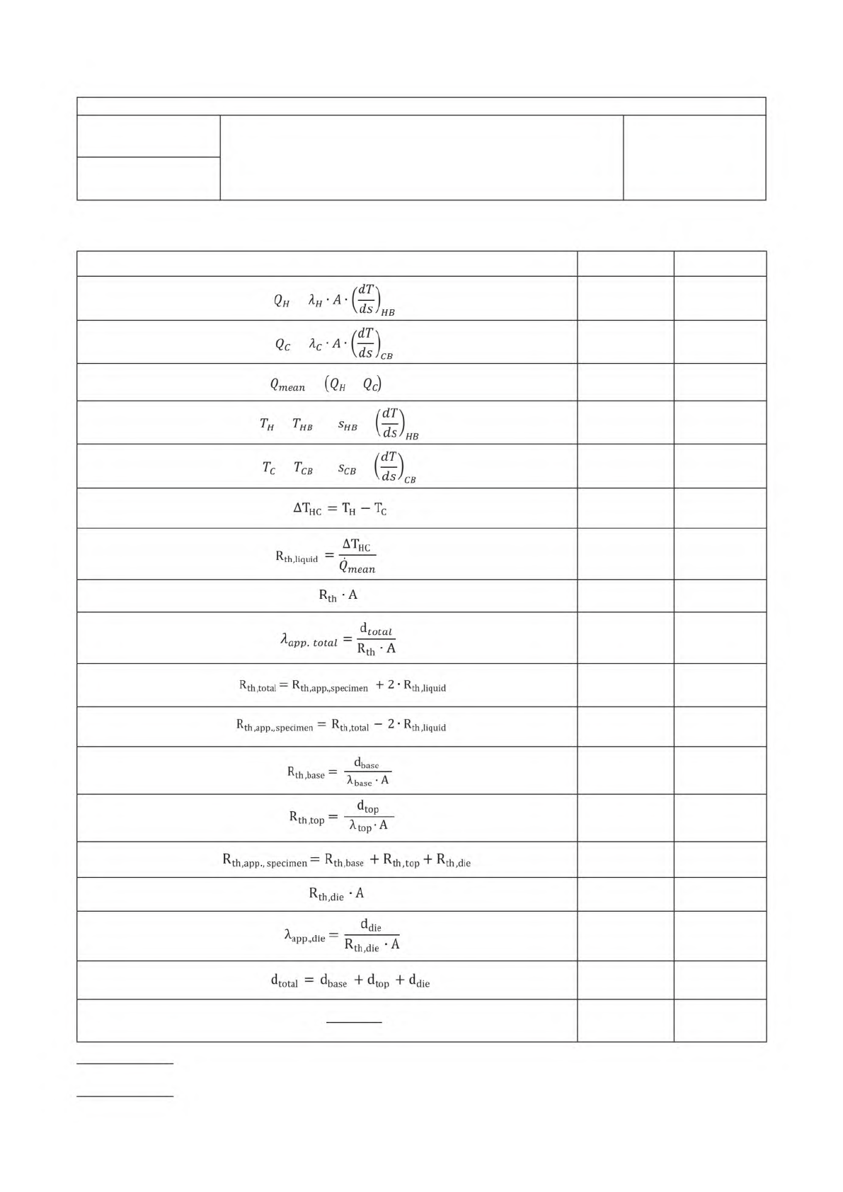
4.13
Use an element that maintains plane parallelism of the specimen and/or
the meter bars themselves (see Figure 3).
4.14
An appropriate device is required to produce the micro section. In order
to generate clean and reproducible results in the form of micro section, the
device must be able to grind and polish the sample (see IPC-TM-650 Test
Methods 2.1.1 or 2.1.1.2).
5 Procedure
5.1
First of all the heating and cooling source should be tempered. Tempering
of the apparatus / the system could have an influence of the measured force
and gap.
5.2
After the apparatus is tempered, tare the force measuring device, when
the heat flow meter bars do not touch.
5.3
After the force is tared, the thickness measuring device needs to be set
to zero as well, if it is implemented in the machine. Otherwise, it has to be
measured before and after measurement. Therefore, the specified surface
pressure should be applied without any specimen between the meter bars.
When the temperature field inside the meter bars is in steady state condition
(∆T/t≤0.2K/300s)thethicknessmeasurementcanbetared.
5.4
Use a liquid like oil or water-glycol to reduce the contact resistance
between the meter bars or the meter bars and the specimen.
5.5
Use asurface pressure of≥ 2.0 N/mm² to reduce the influence ofthe
contact resistances and improve the repeatability of the measurements.
5.6
Measure first the pure liquid (which reduces the contact resistances
between the sample to the meter bars) between the meter bars at the same
surface pressure as the sample (Table 1 Equation 7). From the measured
thermal resistance of the metal based substrate with the used liquid on the
upper and lower side, subtract the measured thermal resistance two times
from this value. See Equations 10 and 11 in Table 1.
5.7
Werecommendhavingatemperaturedifference∆Tacrossthesample≥
1.5 K to reduce the uncertainty. Measure below the glass transition point (TG)
toavoidnonlinearbehavior.Showthemiddletemperature,the∆Tacrossthe
sample and the uncertainty in the results file.
5.8
The measured values are the apparent thermal resistance of the stack
(e.g., Al-die-Cu) (Table 1 Equation 11). Show the results of the thermal
resistance in the dimension (mm²K)/W (Table 1 Equation 8) and the total
apparent thermal conductivity in W/(mK) (Table 1 Equation 9).
5.9
In order to get the apparent thermal conductivity and the thermal resistance
of the dielectric layer between top and base plate of the sample, it is necessary
to know the layer thicknesses of every sample layer. To measure these
thicknesses a microsection of the sample must be made (see IPC-TM-650
Test Methods 2.1.1 or 2.1.1.2 and Table 1 Equation 14). With
known thermal conductivities of the base and top plate of the sample (show in the results the assumed thermal
conductivity of the metals), the thermal resistances of these layers can be determined (Table 1 Equations 12
and 13). With a subtraction of the determined resistances from the apparent thermal resistance of the specimen,
the thermal resistance of the dielectric layer (incl. thermal contact resistances) can be determined (Table 1
1
2
3
Figure3ElementtoMaintainthePlaneParallelismof
theSpecimen
Note1 – Hot Meter Bar
Note2 – Specimen
Note3 – Cold Meter Bar
1
2
4
5
7
6
4
3
Figure4OrderofMaterialsintheMeasuringSection
(incl.theliquid)andSubstituteImageRegardingthe
ThermalResistances
Note1 – Hot Meter Bar
Note2 – Specimen
Note3 – Cold Meter Bar
Note4 – Liquid to Reduce
the Thermal
Contact
Resistances
Note5 – R
th,liquid
Note6 – R
th,specimen
Note7 – R
th,liquid
IPC-TM-650
Number Subject Date
Revision
Page 6 of 7
2.4.54
TestMethodforThermalTransmissionPropertiesof
09/2022
MetalBasedPrintedBoards(MBPB)
N/A
Equation 14). With the thickness from the microsection it is possible
to calculate the apparent thermal conductivity of the dielectric
layer (Table 1 Equation 16). This calculated value must be shown
in the measurement report including the dimensions (mm²K/W)
(Table 1 Equation 15) as well as the apparent thermal conductivity
in W/(mK) (Table 1 Equation 16) and the thicknesses in µm.
5.10
Measure three identical samples across the board and list
all results in the measurement report. In addition, the mean value
and the standard deviation must be listed as well in the report.
5.11
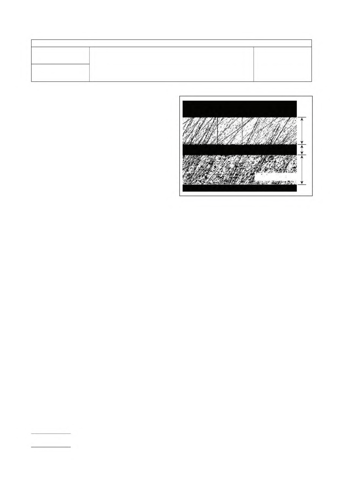
To measure the DIE thickness a cross section according to
IPC-TM-650 Test Method 2.1.1 should to be made.
5.12
To embed the sample, the specimen is first cut in half using
a e.g., metal saw. Afterwards the specimen gets embedded,
grinded and polished.
5.13
The thicknesses of the top and dielectric layer are measured
in the microsection on five different points using a microscope.
Calculate the middle value of the five measured values for each
layer. From the total thickness of the sample, the thickness of
the base layer can be determined by subtraction (see Table 1
Equation 17).
1
2
3
Figure5LayerStructureofaMetal-BasedBoard
Note1: Top layer: d
top,
see 1.3.1
Note2: Dielectric layer: d
die
Note3: Base layer: d
base