IPC-TM-650 EN 2022 试验方法--.pdf - 第500页
Z S S S S S S / Z Z / / S S / S Figure 3 Impedance magnitude (circles) and phase (triangles) for a 25 µm thick dielectric film w ith of 10 and 0.1 1 10 0.01 0.1 1 10 100 - 1 00 -80 -60 -40 -20 0 20 40 60 80 1 00 |Z|= 0.05…
S
S S
Z
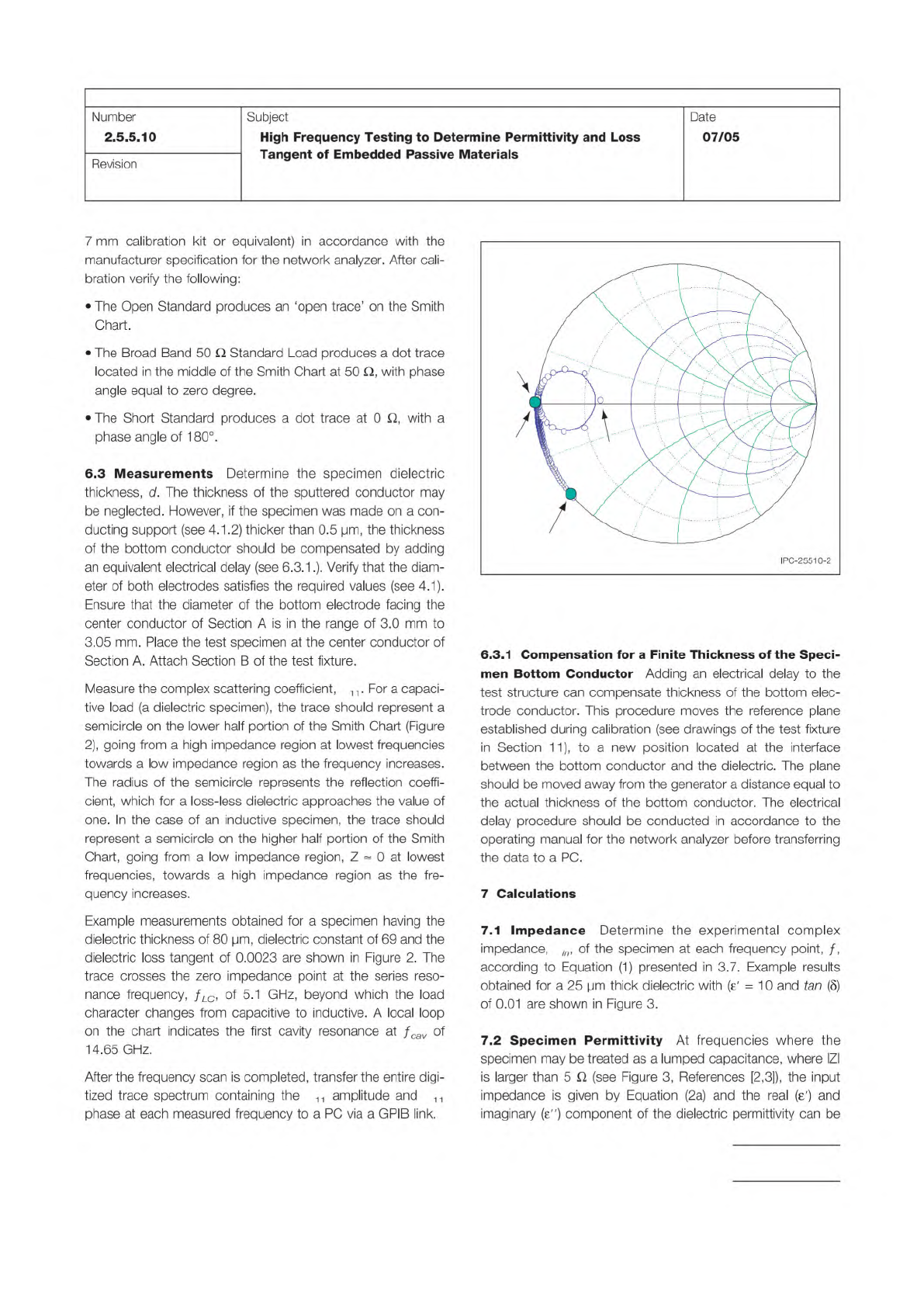
Figure 2 Example measurements plotted in a Smith chart
Format for an 80 µm thick specimen with permittivity of 69
- j0.16.
0.8 1.5 3.0 7.5
-0.8j
0.8j
-1.5j
1.5j
-3.0j
3.0j
-7.5j
7.5j
100 MHz
5.1 GHz
14.65 GHz
Z
in
~
0
~
IPC-TM-650
Page 3 of 8
Number
2.5.5.10
Subject
High
Frequency
Testing
to
Determine
Permittivity
and
Loss
Tangent
of
Embedded
Passive
Materials
Date
07/05
Revision
7
mm
calibration
kit
or
equivalent)
in
accordance
with
the
manufacturer
specification
for
the
network
analyzer.
After
cali¬
bration
verify
the
following:
•
The
Open
Standard
produces
an
'open
trace'
on
the
Smith
Chart.
•
The
Broad
Band
50
Q
Standard
Load
produces
a
dot
trace
located
in
the
middle
of
the
Smith
Chart
at
50
Q,
with
phase
angle
equal
to
zero
degree.
•
The
Short
Standard
produces
a
dot
trace
at
0
Q,
with
a
phase
angle
of
1
80°.
6.3
Measurements
Determine
the
specimen
dielectric
thickness,
d.
The
thickness
of
the
sputtered
conductor
may
be
neglected.
However,
if
the
specimen
was
made
on
a
con¬
ducting
support
(see
4.1.2)
thicker
than
0.5
pm,
the
thickness
of
the
bottom
conductor
should
be
compensated
by
adding
an
equivalent
electrical
delay
(see
6.3.
1.).
Verify
that
the
diam¬
eter
of
both
electrodes
satisfies
the
required
values
(see
4.1).
Ensure
that
the
diameter
of
the
bottom
electrode
facing
the
center
conductor
of
Section
A
is
in
the
range
of
3.0
mm
to
3.05
mm.
Place
the
test
specimen
at
the
center
conductor
of
Section
A.
Attach
Section
B
of
the
test
fixture.
Measure
the
complex
scattering
coefficient,
For
a
capaci¬
tive
load
(a
dielectric
specimen),
the
trace
should
represent
a
semicircle
on
the
lower
half
portion
of
the
Smith
Chart
(Figure
2),
going
from
a
high
impedance
region
at
lowest
frequencies
towards
a
low
impedance
region
as
the
frequency
increases.
The
radius
of
the
semicircle
represents
the
reflection
coeffi¬
cient,
which
for
a
loss-less
dielectric
approaches
the
value
of
one.
In
the
case
of
an
inductive
specimen,
the
trace
should
represent
a
semicircle
on
the
higher
half
portion
of
the
Smith
Chart,
going
from
a
low
impedance
region,
Z
«
0
at
lowest
frequencies,
towards
a
high
impedance
region
as
the
fre¬
quency
increases.
Example
measurements
obtained
for
a
specimen
having
the
dielectric
thickness
of
80
pm,
dielectric
constant
of
69
and
the
dielectric
loss
tangent
of
0.0023
are
shown
in
Figure
2.
The
trace
crosses
the
zero
impedance
point
at
the
series
reso¬
nance
frequency,
fLC,
of
5.1
GHz,
beyond
which
the
load
character
changes
from
capacitive
to
inductive.
A
local
loop
on
the
chart
indicates
the
first
cavity
resonance
at
/cav
of
14.65
GH
乙
After
the
frequency
scan
is
completed,
transfer
the
entire
digi¬
tized
trace
spectrum
containing
the
amplitude
and
口
phase
at
each
measured
frequency
to
a
PC
via
a
GPIB
link.
6.3.1
Compensation
for
a
Finite
Thickness
of
the
Speci¬
men
Bottom
Conductor
Adding
an
electrical
delay
to
the
test
structure
can
compensate
thickness
of
the
bottom
elec¬
trode
conductor.
This
procedure
moves
the
reference
plane
established
during
calibration
(see
drawings
of
the
test
fixture
in
Section
11),
to
a
new
position
located
at
the
interface
between
the
bottom
conductor
and
the
dielectric.
The
plane
should
be
moved
away
from
the
generator
a
distance
equal
to
the
actual
thickness
of
the
bottom
conductor.
The
electrical
delay
procedure
should
be
conducted
in
accordance
to
the
operating
manual
for
the
network
analyzer
before
transferring
the
data
to
a
PC.
7
Calculations
7.1
Impedance
Determine
the
experimental
complex
impedance,
in,
of
the
specimen
at
each
frequency
point,
/,
according
to
Equation
(1)
presented
in
3.7.
Example
results
obtained
for
a
25
pm
thick
dielectric
with
(o'
=
1
0
and
tan
(5)
of
0.01
are
shown
in
Figure
3.
7.2
Specimen
Permittivity
At
frequencies
where
the
specimen
may
be
treated
as
a
lumped
capacitance,
where
IZI
is
larger
than
5
Q
(see
Figure
3,
References
[2,3]),
the
input
impedance
is
given
by
Equation
(2a)
and
the
real
and
imaginary
(£〃)
component
of
the
dielectric
permittivity
can
be
Z
S
S S
S
S
S
/
Z
Z
/
/
S
S / S
Figure 3 Impedance magnitude (circles) and phase
(triangles) for a 25 µm thick dielectric film with
of 10
and
0.1 1 10
0.01
0.1
1
10
100
-
1
00
-80
-60
-40
-20
0
20
40
60
80
1
00
|Z|= 0.05
|Z|= 5
Frequency, GHz
Phase (degree)
|Z|= ( )
IPC-TM-650
Page 4 of 8
Number
2.5.5.10
Revision
Subject
High
Frequency
Testing
to
Determine
Permittivity
and
Loss
Tangent
of
Embedded
Passive
Materials
Date
07/05
g,
tan
(8)
of
0.01.
obtained
directly
from
Equations
(2b)
and
(2c)
respectively
Reference
[2]:
§
1
'n
WCpJ
(2a)
,
-2|
wising
E
=
coZgCp
(1
+
2|
i/cos
,
+
|
nF)
(2b)
1
-
I
nl2
tan
8r
=—=
—
;
——
;
e
-2
1
wising
(2c)
where
|
"
is
the
magnitude
and
(
|)
is
the
phase
of
the
scat¬
tering
coefficient,
co
=
2
兀
/
is
the
angular
frequency,
and
Cp
is
the
specimen
geometrical
(air
filled)
capacitance
(in
units
of
farads),
Cp
=
%
(
兀
a?
4c/)
[F]
(3)
a
is
the
specimen
diameter,
and
d
is
the
dielectric
thickness
of
the
specimen
(in
units
of
meters).
Permittivities
e0
and
%*
are
defined
in
3.1
and
3.2.
In
Equation
(3),
the
specimen
diameter
a
=
3.0
x
10-3
m
(3.0
mm),
should
match
the
diam¬
eter
of
the
central
conductor
pin
(see
4.1
,
Figure
1).
Note
that
the
actual
diameter
of
the
top
electrode
may
be
between
2.85
x
1
0-3
m
to
3.0
x
10-3
m
(2.85
mm
to
3.0
mm
in
4.1).
decreases
to
about
one
tenth
(0.1)
of
the
characteristic
impedance
of
the
coaxial
line,
i.e.,
about
5
Q.
In
the
example
given
in
Figure
3,
this
upper
frequency
limit
is
about
1
.5
GHz.
Some
practical
considerations
regarding
this
limitation
are
dis¬
cussed
in
References
[4
and
5].
At
higher
micro
wave
frequencies,
the
specimen
section
filled
with
a
high-k
material
represents
a
network
of
a
transmission
line
with
capacitance
C
卢;.
The
input
impedance,
fn,
of
such
network
is
given
by
Equation
(4)
(see
Reference
[6]).
Ls
is
the
specimen
residual
inductance,
Ls
=
1.27
10-7[H
(5)
and
the
propagation
term
x
is
given
by
(6):
x
=
co/a/e*
2c
(6)
where,
I
=
2.47
x
10-3
m
(2.47
mm)
represents
the
propaga¬
tion
length
in
the
specimen
section
and
c
is
speed
of
light
(c
二
2.99792
108
m/s).
At
low
frequencies,
below
series
reso¬
nance
frequency,
fLC,
the
propagation
term
x
cot
(x)
approaches
1
,
Ls
can
be
neglected
and
Equation
(4)
simplifies
to
well
known
formula
(2a)
for
a
shunt
capacitance,
Cp&*,
ter¬
minating
a
transmission
line.
7.3
Computational
Algorithm
for
Permittivity
Combin¬
ing
Equations
(1)
and
(4)
leads
to
Equation
(7)
that
relates
the
dielectric
permittivity,
&*,
of
the
test
specimen
with
the
mea¬
surable
scattering
parameter
1
〕
.
*
xcot
(x)
%
」
3Cq
(Zo
(1
+
11)
(1-
11)-/
4)
Because
the
propagation
term
x
depends
on
permittivity
(Equation
(6)),
Equation
(7)
needs
to
be
solved
iteratively.
Description
of
a
suitable
procedure
can
be
found
in
the
Ref¬
erence
[7].
According
to
the
Reference
[7],
the
right-hand-side
of
(7)
can
be
labeled
as
(p
and
rearranged
into
a
compact
form
(7a),
which
is
more
convenient
in
describing
the
iterative
procedure
shown
below.
。
=
Q
(£*)
(7a)
In
practice,
the
conventional
formulas
(2a
-
c)
are
accurate
up
to
a
frequency
at
which
the
input
impedance
of
the
specimen
/
S
/
S
Z
IPC-TM-650
Page 5 of 8
Number
2.5.5.10
Subject
High
Frequency
Testing
to
Determine
Permittivity
and
Loss
Tangent
of
Embedded
Passive
Materials
Date
07/05
Revision
For
each
frequency
repeat
the
following
procedure:
1
.
Compute
the
complex
permittivity
using
Equations
(2b)
and
(2c).
This
is
an
initial
trial
solution
of
the
iterative
process
for
k=0,
where
k
is
the
iterative
step:
£
;
[k
=
0]
=
V
-尤"
(
7b)
2.
Compute
successive
approximations
for
subsequent
itera¬
tive
steps
k.
A
[k
+
1
]
=
<p
(J
[k])
(7c)
(k
=
0,
1
,
2,
3...)
3.
The
iteration
procedure
is
terminated
when
the
absolute
value
of
Equation
(7d)
is
sufficiently
small,
for
example
smaller
than
1
0-5.
|E;W-£;[k-1]|
|e;W|<10-5
(7d)
Typically
it
may
require
five
to
about
twenty
iterations
to
reach
the
terminating
criterion.
Commercially
available
software
can
be
used
to
program
and
automate
the
computational
steps
1
through
3
and
solve
Equation
(7)
numerically
for
e*
and
the
corresponding
uncer¬
tainty
values.
The
software
should
be
capable
of
handling
simultaneously
both
real
and
imaginary
parts
of
complex
〕
〔
,
x
cot
(x)
and
£*,
(for
example
Visual
Basic,
C
or
Agilent
VEE
and
National
Instruments
LabView
programming
platforms
can
be
employed).
8
Report
The
report
shall
include:
•
Dimensions
of
the
specimen.
•
Plot
of
magnitude
and
phase
of
the
measured
impedance
as
a
function
of
frequency,
(similar
to
Figure
3)
or
Smith
Chart.
•
Plot
of
£'
and
U'
or
ez
and
tan
8
as
a
function
of
frequency.
9
Notes
9.1
Measurements
at
Frequency
Range
Above
12
GHz
The
presented
APC-7
test
fixture
design
may
be
utilized
in
the
frequency
range
of
100
kHz
to
18
GHz.
The
computational
algorithm
and
in
particular
Equations
(4)
and
(5)
have
been
validated
up
to
the
first
cavity
resonance
frequency,
fcav,
which
is
determined
by
the
propagation
length
/,
and
the
dielectric
constant
of
the
specimen:
fcav
=
^-7=
~
1
21
N%
[GHz]
I
Re
(\e^)
(8)
where
Re
indicates
the
real
part
of
complex
square
root
of
permittivity
and
/
=
2.47
mm,
which
is
the
propagation
length
for
the
test
fixture
presented
in
Figure
1,
[5].
For
example,
in
the
case
of
a
specimen
having
the
dielectric
constant
of
1
00
fcav
is
about
1
2
GHz.
9.2
Accuracy
Considerations
Several
uncertainty
factors
such
as
instrumentation,
dimensional
uncertainty
of
the
test
specimen
geometry,
roughness
and
conductivity
of
the
con¬
duction
surfaces
contribute
to
the
combined
uncertainty
of
the
measurements.
The
complexity
of
modeling
these
factors
is
considerably
higher
within
the
frequency
range
of
the
LC
reso¬
nance.
Adequate
analysis
can
be
performed,
however,
by
using
the
partial
derivative
technique
[1]
for
Equations
(2b)
and
(2c)
and
considering
the
instrumentation
and
the
dimensional
errors.
The
standard
uncertainty
of
「
can
be
assumed
to
be
within
the
manufacturer's
specification
for
the
network
ana¬
lyzer,
about
±
0.005
dB
for
the
magnitude
and
土
0.5°
for
the
phase.
The
combined
relative
standard
uncertainty
in
geo¬
metrical
capacitance
measurements
is
typically
better
than
5%,
where
the
largest
contributing
factor
is
the
uncertainty
in
the
film
thickness
measurements.
Equation
(5)
for
the
residual
inductance
has
been
validated
for
specimens
8
pm
to
300
pm
thick.
However,
since
residual
inductance
becomes
smaller
with
thinner
dielectrics,
mea¬
surements
can
be
accurately
made
for
sample
thicknesses
down
to
1
pm.
Measurements
in
the
frequency
range
of
100
MHz
to
12
GHz
are
reproducible
with
relative
combined
uncertainty
in
£'
and
of
better
than
8%
for
specimens
having
e(
<80
and
thick¬
ness
d
<300
pm.
The
resolution
in
the
dielectric
loss
tangent
measurements
is
<0.005.
Additional
limitations
may
arise
from
the
systematic
uncer¬
tainty
of
the
particular
instrumentation,
calibration
standards
and
the
dimensional
imperfections
of
the
actually
imple¬
mented
test
fixture.
Results
may
be
not
reliable
at
frequencies
where
| |
decreases
below
0.05
Q,
which
in
Figure
3
is
shown
as
a
frequency
range
of
11
.9
GHz
to
1
3.5
GHz.
9.3
Test
Software
Test
software
enabling
this
technique
to
be
performed
is
available
in
the
Agilent
VEE
platform.
Please
contact
Dr.
Jan
Obrzut
at
NIST-Gaithersburg,
MD
(jan.obrzut@nist.gov)
to
obtain
such.
9.4
Metric
Units
of
Measure
This
test
method
uses
only
metric
units
of
measure,
as
is
the
case
with
nearly
all
such
high
frequency
test
methods.
Conversion
to
English/lmperial
units
has
not
been
done
in
this
document,
as
any
conversions