IPC-TM-650 EN 2022 试验方法--.pdf - 第503页
IPC-TM-650 Page 2 of 2 Number 2.5.7.1 Subject Dielectric Withstanding Voltage - Polymeric Conformal Coating Date 07/00 Revision 5.1.2 Immerse and agitate the test specimens in 2-propanol for 30 seconds. Scrub with a soft…
http://
physics.nist.gov/cgi-bin/cuu/Value?ep0|search_for=permittivity
6
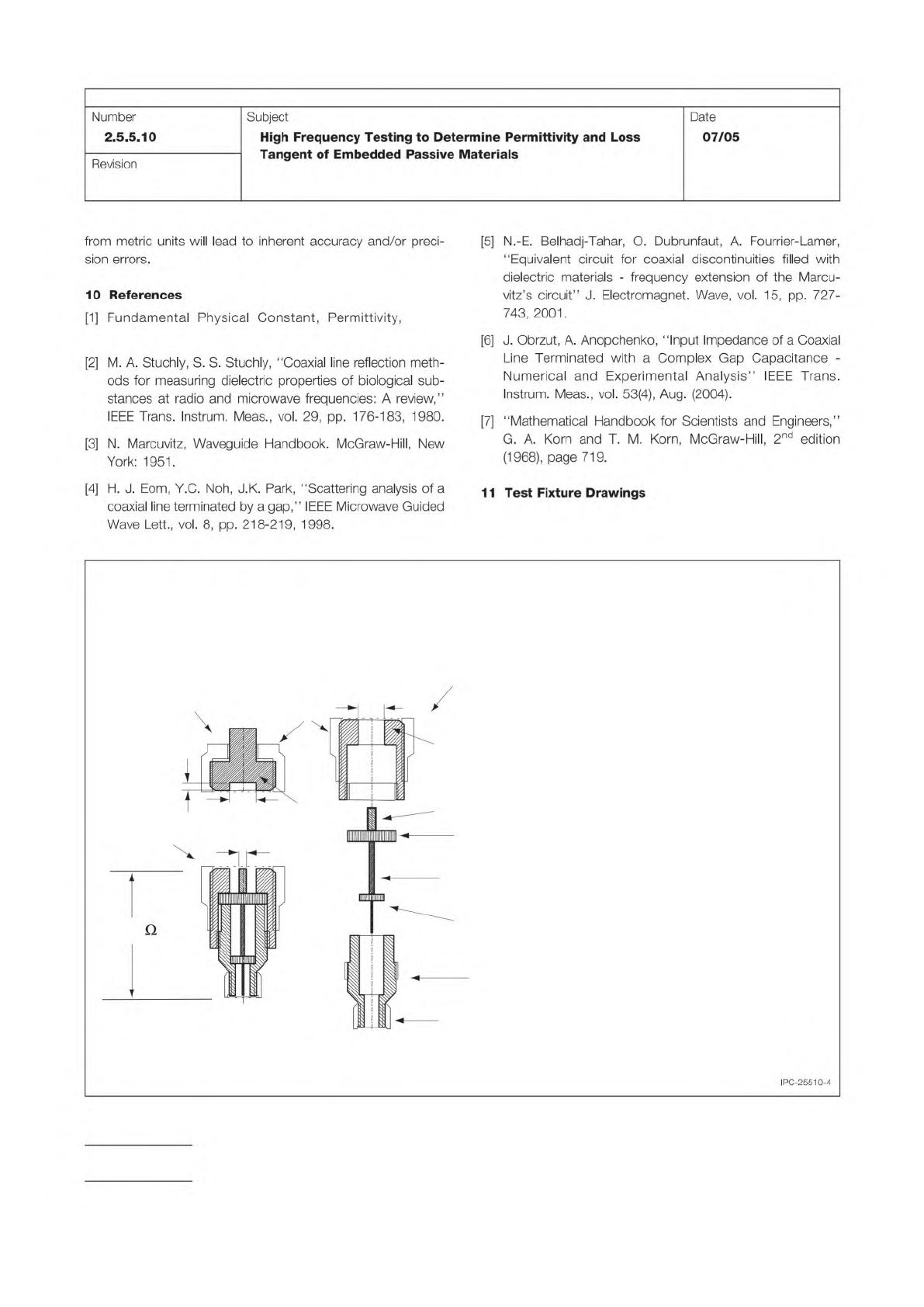
1 Center conductor pin
a
= 3.05 mm
2 Supporting dielectric in the APC-7 section
3 Center conductor in the APC-7 to APC-3.5
4 Supporting dielectric in the APC-3.5 section
5 APC-3.5 section of the adaptor
6 Section A outer conductor (
b
=7.00 mm)
7 Section B outer conductor (
b
=7.00 mm)
8 APC-7 mount
8
1
2
a
d
b
b
Section B
Section A
Section A details
Test Fixture for HF Permittivity of Embedded Passive Materials
Originator: IPC Embedded Passives Test Methods
3
4
5
50
Calibration Plane
METRIC, dimensions are in mm
7
APC-3.5 female mount
IPC-TM-650
Page 6 of 8
Number
2.5.5.10
Subject
High
Frequency
Testing
to
Determine
Permittivity
and
Loss
Tangent
of
Embedded
Passive
Materials
Date
07/05
Revision
from
metric
units
will
lead
to
inherent
accuracy
and/or
preci¬
sion
errors.
10
References
[1]
Fundamental
Physical
Constant,
Permittivity,
[2]
M.
A.
Stuchly,
S.
S.
Stuchly,
"Coaxial
line
reflection
meth¬
ods
for
measuring
dielectric
properties
of
biological
sub¬
stances
at
radio
and
microwave
frequencies:
A
review,”
IEEE
Trans.
Instrum.
Meas.,
vol.
29,
pp.
176-183,
1980.
[3]
N.
Marcuvitz,
Waveguide
Handbook.
McGraw-Hill,
New
York:
1951.
[4]
H.
J.
Eom,
Y.C.
Noh,
J.K.
Park,
"Scattering
analysis
of
a
coaxial
line
terminated
by
a
gap,”
IEEE
Microwave
Guided
Wave
Lett.,
vol.
8,
pp.
218-219,
1998.
[5]
N.-E.
Belhadj-Tahar,
O.
Dubrunfaut,
A.
Fourrier-Lamer,
"Equivalent
circuit
for
coaxial
discontinuities
filled
with
dielectric
materials
-
frequency
extension
of
the
Marcu-
vitz's
circuit”
J.
Electromagnet.
Wave,
vol.
15,
pp.
727-
743,
2001.
[6]
J.
Obrzut,
A.
Anopchenko,
'Input
Impedance
of
a
Coaxial
Line
Terminated
with
a
Complex
Gap
Capacitance
-
Numerical
and
Experimental
Analysis”
IEEE
Trans.
Instrum.
Meas.,
vol.
53(4),
Aug.
(2004).
[7]
"Mathematical
Handbook
for
Scientists
and
Engineers,”
G.
A.
Korn
and
T.
M.
Korn,
McGraw-Hill,
2nd
edition
(1968),
page
719.
11
Test
Fixture
Drawings
IPC-25510-4
IPC-TM-650
Page 2 of 2
Number
2.5.7.1
Subject
Dielectric
Withstanding
Voltage
-
Polymeric
Conformal
Coating
Date
07/00
Revision
5.1.2
Immerse
and
agitate
the
test
specimens
in
2-propanol
for
30
seconds.
Scrub
with
a
soft
bristle
brush
and
spray
with
clean
2-propanol.
5.1.3
Place
the
cleaned
specimens
in
an
oven
maintained
at
50℃
[1
22°F]
for
three
to
five
hours
to
dry.
5.1.4
Remove
the
specimens
from
the
oven
and
place
in
a
desiccator
to
cool.
5.1.5
Conformal
coat
the
test
specimens
and
cure
in
accor¬
dance
with
the
suppliers
recommendations.
If
the
specimens
are
not
used
immediately,
seal
the
specimens
in
Kapac®
bags.
5.2
Procedure
5.2.1
For
each
individual
specimen,
secure
all
the
positive
leads
(1
,
3
and
5)
together
and
the
negative
(2
and
4)
together.
5.2.2
Attach
the
leads
of
the
Hi-Pot
Tester
to
the
wires
of
the
test
specimen.
5.2.3
Raise
the
test
voltage
from
zero
to
1,500
VAC
at
1
00
VAC
per
second.
5.2.4
Apply
the
test
voltage
of
1
,500
VAC
at
50-60
Hz
for
one
minute
and
record
any
leakage
rate.
5.2.5
After
the
one-minute
duration,
turn
off
the
voltage
and
disconnect
the
test
specimen
from
the
Hi-Pot
Tester.
6.0
Evaluate
6.1
Record
if
the
specimen
exhibits
flashover,
sparkover
or
breakdown.
6.1.1
Record
the
leakage
current
of
each
specimen.
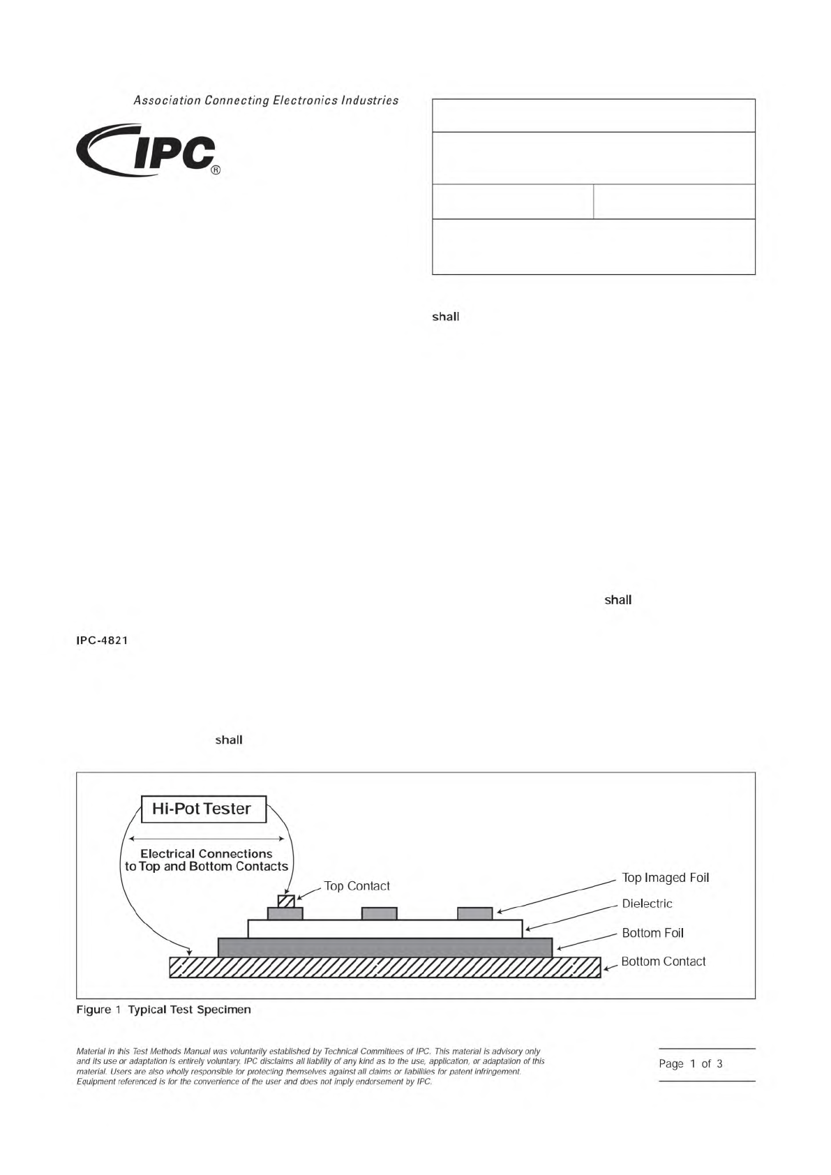
1 Scope
The dielectric withstanding voltage test (Hipot test)
consists of the application of a voltage higher than the oper-
ating voltage for a specific time across the thickness of the
test specimen’s dielectric layer. This is used to prove that a
printed board can operate safely at its rated voltage and with-
stand momentary voltage spikes due to switching, surges,
and other similar phenomena. Although this test is similar to a
voltage breakdown test, it is not intended for this test to cause
insulation breakdown. Rather, it serves to determine whether
the test specimen’s layers have adequate withstanding volt-
age. This document is applicable to thin dielectric materials
such as those defined by IPC-4821.
The results can be indicative of a change or a deviation from
the normal material characteristics resulting from manufactur-
ing, processing or aging conditions. The test is useful for qual-
ity acceptance and in the determination of the suitability of the
material for a given application and may be adapted for pro-
cess control.
2 Applicable Documents
Specification for Embedded Passive Device
Capacitor Materials for Rigid and Multilayer Printed Boards
3 Test Specimen
3.1 Qualification Testing
For laminate-like capacitor
materials, test specimens
be 50 mm [1.97 in] diameter
circular electrodes (see ‘‘Top Imaged Foil’’ in Figure 1) that
be formed by imaging and then etching the copper foil,
unless otherwise as agreed upon by user and supplier
(AABUS). Spacing between adjacent Top Imaged Foil con-
ductors is recommended to be ≥100 times the dielectric thick-
ness. In order to avoid field gradient and mechanical stress
concentration, which can cause faulty dielectric breakdown,
the Bottom Foil can be either a circle larger than the Top
Imaged Foil or can be a continuous copper sheet. The con-
tinuous copper sheet will be required for very thin capacitor
dielectric layers that are not self-supporting.
For nonlaminate-like capacitor materials, the test specimen’s
Top Imaged Foil can be a size other than a 50 mm [1.97 in]
diameter circle, if this size is not practical or typical. The test
specimen’s Top Imaged Foil size for these nonlaminate-like
materials should be set to the largest size normally recom-
mended for this product (see 5.2.4). The thickness for the test
specimens should be the typical/recommended thickness. A
minimum of five test specimens
be tested for qualifica-
tion.
3.2 Conformance Testing
Test specimens can be the
same as used for qualification testing or can be other sizes or
shapes. For testing in printed board environments, actual
innerlayer power and ground features are typically used,
although other board features or test specimens can also be
used. Please note that adjustments for capacitor plate size are
required in the test procedure (see Section 6).
IPC-2572-1.eps
3000 Lakeside Drive, Suite 309S
Bannockburn, IL 60015-1249
IPC-TM-650
TEST METHODS MANUAL
Number
2.5.7.2
Subject
Dielectric Withstanding Voltage (Hipot Method) -
Thin Dielectric Layers for Printed Boards
Date
11/2009
Revision
A
Originating Task Group
Embedded Devices Test Methods Subcommittee
(D-54)
Association
Connecting
Electronics
Industries
shall
IPC-4821
shall
shall
Top
Imaged
Foil
Dielectric
Bottom
Foil
Bottom
Contact
Figure
1
Typical
Test
Specimen
Material
/n
this
Test
Methods
Manual
was
voluntarily
established
by
Technical
Committees
of
I
PC.
This
material
/s
advisory
only
and
"s
use
or
adaptation
,
s
entirely
voluntary.
IPC
disclaims
all
liability
of
any
kind
as
to
the
use,
application,
or
adaptation
of
this
material.
Users
are
also
wholly
responsible
for
protecting
themselves
against
all
claims
or
liabilities
for
patent
infringement.
Equipment
referenced
/s
for
the
convenience
of
the
user
and
does
not
imply
endorsement
by
IPC.
Page
1
of
3