IPC-TM-650 EN 2022 试验方法--.pdf - 第539页
V1(f) and V2(t) is a respective ordered frequency pair A 1 (f) , φ 1 (f) and A 2 (f) , φ 2 (f) . The atte nuation, Att(f) , and phase constant, β (f) , ar e com- puted w ith Equ ations 5- 10 an d 5-11. Γ( , ) = α( , ) + …
If bolting the SMA connectors on in free space, one needs to
position the DUT to ensure the maximum peak signal.
5.3.6.1 SPP Signal Processing
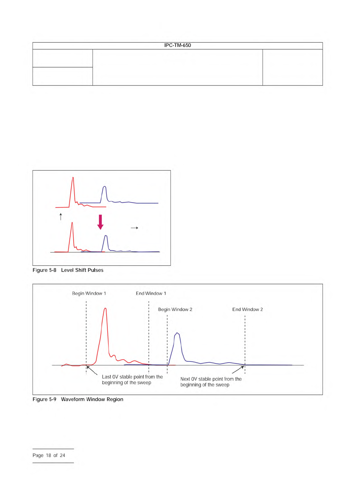
5.3.6.1.1 Level Shifting
The first step is to shift the two
pulses to a common level. Both pulses are shifted to a 0V
level as shown in Figure 5-8. Some pulses will have an initial
offset due to excessive DC drop in the system.
5.3.6.1.2 Time Windowing
Time windowing is required
before the subsequent step that uses a Fast Fourier Trans-
form (FFT). The two waveform windows are defined as a
region of time that starts at the last stable point around 0V for
each conductor and ends next to the stable point around 0V
on the long conductor, as illustrated in Figure 5-9. It is recom-
mended to first determine the extent of Window 2 for the long
line and then use the same extent for the short line, such that
Window 1 and Window 2 are identical.
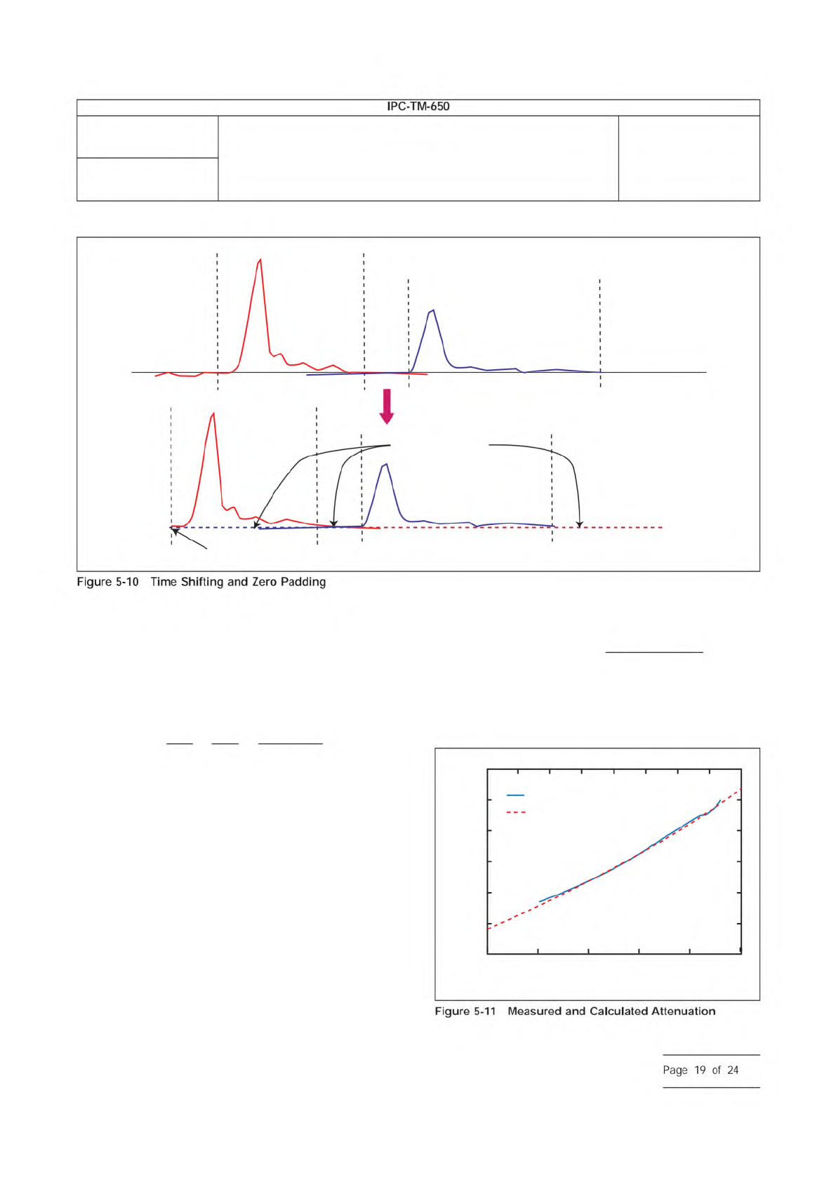
5.3.6.1.3 Time Shifting and Padding
The next step is to
utilize the window to shift both waveforms by the same delay
so that the beginning of Window 1 is at 0 seconds. Subse-
quently all waveform samples not in the windows are set to 0V
and are called padding. Figure 5-10 provides an example.
5.3.6.2 Fourier Transformation
The Fourier transform is
performed on the two time shifted pulses using the same
number of points as were used in the time-shifting and pad-
ding step (this is important). The number of points must be a
power of 2; a typical number of steps is 8192 or 16384.
Re-sampling is normally required to meet this requirement.
V1(t) is the shifted and padded waveform that represents the
short line of length l
1
and V2(t) is the shifted and padded
waveform that represents the long line of length l
2
. The FFT of
IPC-25512-5-8
Time
Voltage
0V
IPC-25512-5-9
Number
2.5.5.12
Subject
Test Methods to Determine the Amount of Signal Loss on
Printed Boards
Date
07/12
Revision
A
IPC-TM-650
Page
18
of
24
V1(f) and V2(t) is a respective ordered frequency pair A1(f),
φ1(f) and A2(f), φ2(f).
The attenuation, Att(f), and phase constant, β(f), are com-
puted with Equations 5-10 and 5-11.
Γ(,) = α(,) + jβ(,) =
−
1
l
1
– l
2
1n
(
A
1
(,)
A
2
(,)
)
+ j
φ
1
(,) − φ
2
(,)
l
1
− l
2
[5-10]
Att(,) = 20 log (e
Re(Γ(,)
)
β(,) = Im (Γ(F))
[5-11]
5.3.6.3 SPP Broadband Complex Permittivity Extraction
5.3.6.3.1 Frequency Dependent Line Parameters
A 2D
field solver is used to calculate R(f), L(f), C(f), and G(f) per unit
length based on the actual cross sectional dimensions, the
metal resistivity ρ, and low frequency ε
r
and tanδ outlined
above. A 2D solver that assures a causally related calculation
of L-R and C-G is recommended. The initial calculation can
contain a few initial points for ε
r
and tanδ that are used as
starting values for the high-frequency range, for example
3 GHz to 20 GHz. Based on the calculated R(f), L(f), C(f), and
G(f), the attenuation and phase constant are calculated from
Equation 5-12.
Γ(,) = α(,) + jβ(,) =
√
(R + jωL)(G + jωC)
[5-12]
The measured and calculated attenuation and phase are
compared to the measured values as shown in Figure 5-11
and Figure 5-12.
IPC-25512-5-10
0V, 0S
Zero Padded
IPC-25512-5-11
Attenuation (dB/cm)
0.05
0.1
0.2
0.5
1
2
5
1 2 5 10 20 50
Frequency (GHz)
Measured
Calculated
Number
2.5.5.12
Subject
Test Methods to Determine the Amount of Signal Loss on
Printed Boards
Date
07/12
Revision
A
IPC-TM-650
—
Figure
5-10
Time
Shifting
and
Zero
Padding
Figure
5-11
Measured
and
Calculated
Attenuation
Page
19
of
24
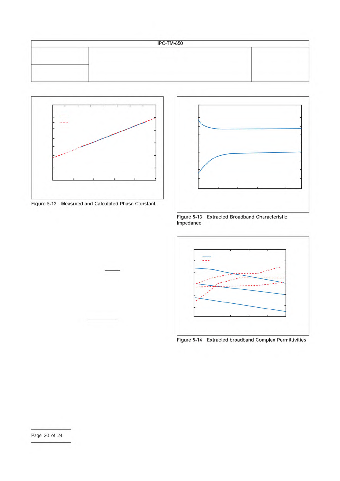
The calculation is iterated until good agreement is obtained.
Agreement is assessed visually. Each time, the high-frequency
values of ε
r
and tanδ are modified. It is recommended to use
a 2D field solver that has a Debye model for the relation
between C and G as described in Equation 5-13 with a large
number of poles to cover a broad frequency range. 30 poles
are considered a good practice.
ε(ω) = ε
∞
+
Σ
i
ε
i
1 + jωτ
i
[5-13]
The solver should be able to smoothly interpolate between the
low frequency values and the high-frequency ones.
The broadband Z
0
(f) is also obtained based on R(f), L(f), C(f),
G(f) as shown in Equation 5-14.
Z
0
=
Γ(ω)
G(ω) + jωC(ω)
[5-14]
An example of such broadband impedance is shown in Figure
5-13.
5.3.6.3.2 Frequency Dependent Complex Permittivity
Extraction
The final R(f), L(f), C(f), and G(f) are used to
extract the complex permittivity using Equation 1-2 and 1-3.
Some examples of extracted permittivities are shown in Figure
5-14.
IPC-25512-5-12
Phase Constant (1/cm)
0.05
0.5
1
2
20
10
5
50
1 2 5 10 20 50
Frequency (GHz)
Measured
Calculated
IPC-25512-5-13
Impedance (Ω)
-80
-60
-40
-20
0
20
40
60
80
100
0.001 0.01 0.1 1 10 50
Frequency (GHz)
Real Zo
Imag Zo
IPC-25512-5-14
Dielectric Constant ε
Dielectic Loss tanδ
3.2
3.4
0.005
0
0.010
0.015
0.020
0.025
0.030
3.6
3.8
2 5
BT
BT
Nelco
Nelco
Nelco
NelcoSI
BT, Nelco 4000–13SI, 6 Layers, 3.75/3.55/3.7
10 20 50
Frequency (GHz)
tan
δ
Number
2.5.5.12
Subject
Test Methods to Determine the Amount of Signal Loss on
Printed Boards
Date
07/12
Revision
A
IPC-TM-650
Figure
5-12
Measured
and
Calculated
Phase
Constant
Figure
5-13
Extracted
Broadband
Characteristic
Impedance
Figure
5-14
Extracted
broadband
Complex
Permittivities
Page
20
of
24