IPC-TM-650 EN 2022 试验方法--.pdf - 第748页
signal-2 vias; for a total of 168 pot ential in-line PTH-PTH fail- ures for each spac ing distance. Holes Staggered (cl osest PTH-PTH spacing in diagonal di rec- tion): There are three rows of 26 signal-1 vias inter mesh…
45° angle results in a square 1.08 mm x 1.08 mm [0.04252 in
x 0.04252 in] grid. Note: the sketches do not look square
when tipped 45° but, the CAF Test Boards do. The resulting
via edge to via edge spacings are: 0.26 mm, 0.37 mm,
0.51 mm, 0.62 mm [0.0102 in, 0.0146 in, 0.0201 in,
0.0244 in]. Other than the use of different drilled hole sizes
and a small change in pad sizes, the four structures are iden-
tical. The vias in the ‘‘B’’ test structure are not aligned with the
glass fibers. If the failure mode is along glass bundles it is rea-
sonable to expect the ‘‘B’’ test structure to perform better
than the ‘‘A’’ structure for equivalent via edge to via edge
spacings. Within a given test structure, the inner and outer
layer pads for all 10 layers are the same, i.e., the same pad
size is consistently used within a given test structure although,
it does change from structure to structure. All via to electrode
connections are made on layer 1 and are repeated on layer 10
so that a single etch-out will not affect results.
A conceptual representation of the ‘‘B’’ test structure of
the coupons in Figure 1 is shown to the upper right.
Design details on each of the four ‘‘B’’ test structures follows
in Table 2.
3.2 Other Structures
Section C is designed to evaluate
plated-through hole (PTH)-to-plane layer spacings. It is rec-
ommended to use the registration coupon per test board (IPC
Test Pattern F) when CAF testing includes this region. Section
D in the IPC-9254 design is for layer-to-layer Z-axis CAF test-
ing. Section D in the IPC-9253 is for evaluating CAF resis-
tance in a press-fit compliant pin connector application. The
feature in the D region is an optional feature that is present
automatically with the design. However, the A, B and C
regions
remain as designed in order to provide a stan-
dard basis of comparison.
The CAF test board with 10 layers is designated to evaluate
thin single-ply constructions typically used on high perfor-
mance boards. This board construction stackup can be
reduced down to: (a) four layers by eliminating layers 3
through 8 and (b) only test structures A and B, when just
evaluating differences between laminate materials.
3.3 CAF Test Board Design
This 10-layer CAF test board
for evaluating the insulation resistance between internal con-
ductors within a printed wiring board has the following key
features for evaluating hole-hole CAF resistance (Figure 3).
Holes In-Line (in-line with glass fiber direction): There are two
rows of 42 signal-1 vias intermeshed with three rows of 42
Outer layer pad size 0.86 mm [0.0339 in] 0.81 mm [0.0319 in] 0.75 mm [0.0295 in] 0.69 mm [0.0272 in]
Inner layer pad size 0.86 mm [0.0339 in] 0.81 mm [0.0319 in] 0.75 mm [0.0295 in] 0.69 mm [0.0272 in]
Drilled hole size 0.74 mm [0.0291 in] 0.63 mm [0.0248 in] 0.51 mm [0.0201 in] 0.37 mm [0.0146 in]
Via edge to via edge
(shortest distance)
0.27 mm [0.0106 in] 0.38 mm [0.0150 in] 0.51 mm [0.0201 in] 0.65 mm [0.0256 in]
Via edge to via edge
(Manhattan Distance)
0.27 mm [0.0106 in] 0.38 mm [0.0150 in] 0.51 mm [0.0201 in] 0.65 mm [0.0256 in]
On IPC-9254
, bias
applied between:
J1, J5 J2, J5 J3, J5 J4, J5
IPC-2625-2
Number
2.6.25
Subject
Conductive Anodic Filament (CAF) Resistance Test: X-Y Axis
Date
02/21
Revision
C
IPC-TM-650
—
Table
1
Test
Structures
A1
through
A4
Design
Rules
A1
A2
A3
A4
only
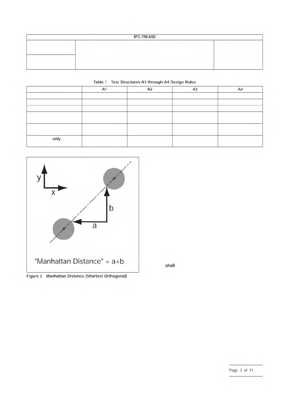
"Manhattan
Distance"
=
a+b
Figure
2
Manhattan
Distance
(Shortest
Orthogonal)
shall
Page
3
of
11
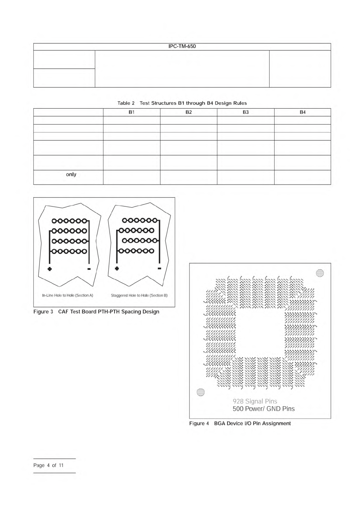
signal-2 vias; for a total of 168 potential in-line PTH-PTH fail-
ures for each spacing distance.
Holes Staggered (closest PTH-PTH spacing in diagonal direc-
tion): There are three rows of 26 signal-1 vias intermeshed
with four rows of 27 signal-2 vias; for a total of 312 potential
diagonal PTH-PTH failures for each spacing distance.
3.4 CAF Test Coupon/Board Quantity
The CAF testing
data analysis technique recommended for either of these CAF
test coupon/board designs requires a minimum 25 CAF test
boards to be run per sample lot per bias level for statistical
significance. This provides a total of 4,200 potential in-line
hole-hole CAF failure sites and 7,800 potential diagonal hole-
hole CAF failure sites for each unique sample/condition set.
For comparison, on a 1,428 I/O BGA device (Figure 4) there
are about 500 power/ground pins. So with an average of
slightly less than two adjacent power/ground pin spacings per
pin there are about 1,000 potential in-line hole-hole CAF fail-
ure sites per BGA device. For a production board with the
equivalent of three of these BGA devices and about 1200
passives or other components with close power/ground pin
spacings, the total number of opportunities for in-line CAF fail-
ure would then be about 4,200 (about the same as the entire
CAF test board sample lot of 25 pieces).
3.5 CAF Test Small Coupon Designs
The IPC-9255 and
IPC-9256 CAF test coupon designs (Figure 5) have 10 layers,
Outer layer pad size 0.94 mm [0.0370 in] 0.89 mm [0.0350 in] 0.84 mm [0.0330 in] 0.75 mm [0.0300 in]
Inner layer pad size 0.94 mm [0.0370 in] 0.89 mm [0.0350 in] 0.84 mm [0.0331 in] 0.75 mm [0.0295 in]
Drilled hole size 0.81 mm [0.0319 in] 0.71 mm [0.0280 in] 0.57 mm [0.0224 in] 0.46 mm [0.0181 in]
Via edge to via edge
(shortest distance)
0.26 mm [0.0102 in] 0.37 mm [0.0146 in] 0.51 mm [0.0201 in] 0.62 mm [0.0244 in]
Via edge to via edge
(Manhattan Distance)
0.37 mm [0.0146 in] 0.52 mm [0.0205 in] 0.72 mm [0.0283 in] 0.88 mm [0.0346 in]
On IPC-9254
, bias
applied between:
J7, J11 J8, J11 J9, J11 J10, J11
IPC-2625-3
IPC-2625-4
Number
2.6.25
Subject
Conductive Anodic Filament (CAF) Resistance Test: X-Y Axis
Date
02/21
Revision
C
IPC-TM-650
―
Table
2
Test
Structures
B1
through
B4
Design
Rules
B1
B2
B3
B4
only
Figure
3
CAF
Test
Board
PTH-PTH
Spacing
Design
曹
///////////<
^:<«««««
必依
依依
2
SSSV
SSSV
%%S*w*
SSSS
、、、y
ssssj
、、、y
、、、、
‘////
、
w
、、、v
、、•
7//
、、W
、、…
*
VASSSW
、、'
、、、w
、、•
///////
SV
、、"
SSSS
•**、、、
A\W
A
、、\
«*•、、、
《*»、、、
入
\W、
Z、、
人
、、、
人
、、、
Z.SSS
人
d
、
A
、、、、」
“/券
、、、
八、
\\
八、、
、
八
'、、
八
、、、、*>///
*.•,<**
八、
八、
、、
人、
、、
人、
\\
人%
、\
人、
、\
8
5、
/////
,W,4
,、
Z*、、、
A
、、\
A
、、、
z*sw
八、
、、
八、、
//////
«<<<«««
八
、、、
人、
、、
《*»、、、
八、
、、
八、
八
、
///////
女箭
£5
多&
然
今避
然
交送
多浏
浏沪
<<><<<><>>>,%
•**、、、
八
、、、
A
、\
///////////
«*.*,*,*.«*.<*.*.
////////////
s»x
r
、、
a
、、
Z*
黑&
s
〉>>>>〉
〉八
、、、▼
、、、▼ 、、、▼
55555555
、、w 、、w
、、、V
»»»»»
/
/
、、W
、、W
、、W
、"
、、、w*
、、、D
、、、▼
、、//»〃
、、、v
、、
w
、、、v
、、、<f
、、W 、、W
、、
W
NSSS
、、w
、、w
、、w
、、、、
?
乃坡
坡乃乃
p
////////////
////////////
城浏
浏浏夕
////////////
»»»»»>^
////////////
////////////
////////////
数为
2
坡坡
以
7
928
Signal
Pins
500
Power/
GND
Pins
Figure
4
BGA
Device
I/O
Pin
Assignment
Page
4
of
11
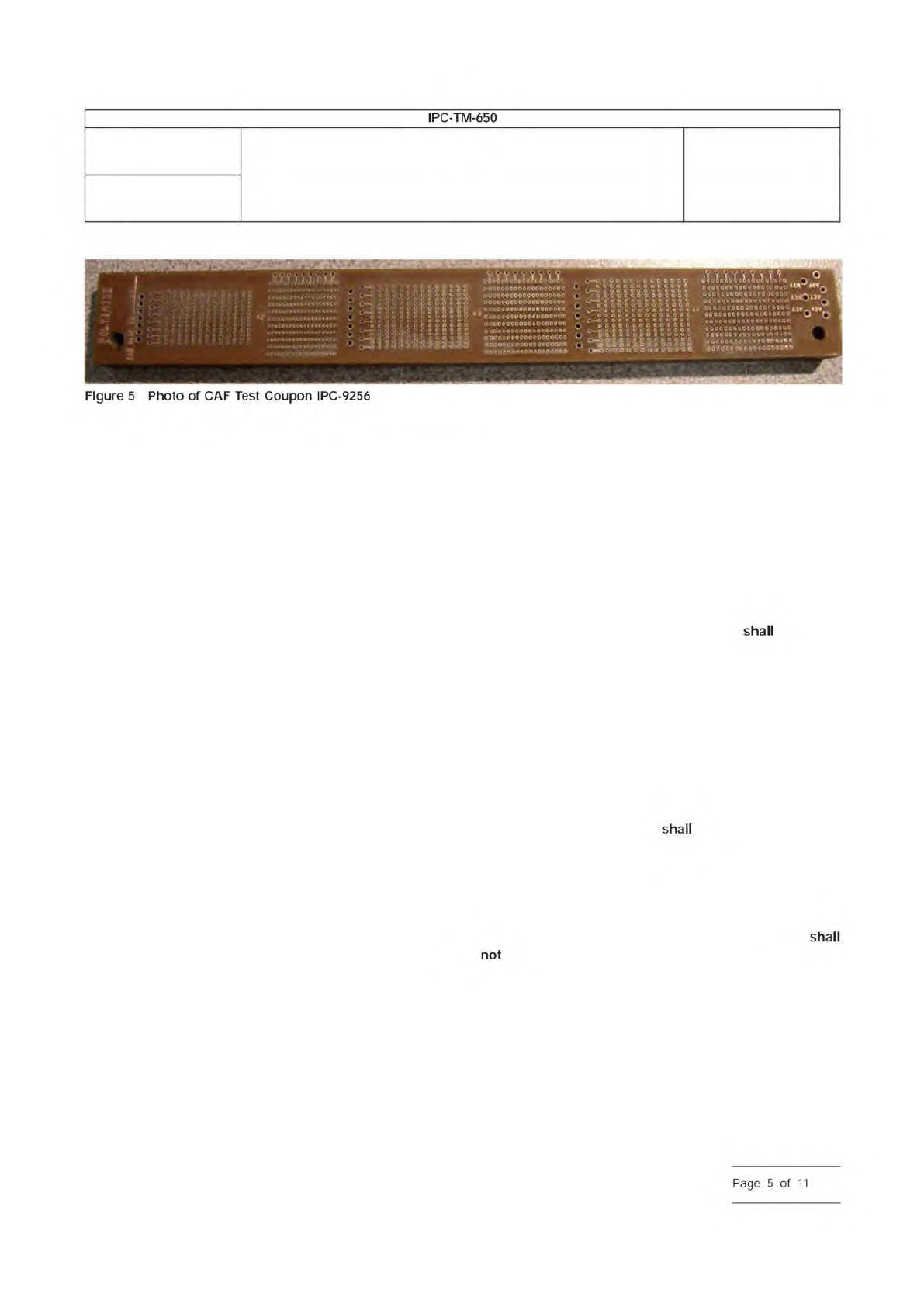
each approximately 0.7 in x 5 in. Layers 5 and 6 have no trace
routing, so removing them provides an 8 layer coupon. Con-
versely, by duplicating layers 5 and 6, a 14-layer or higher
layer count coupon can be obtained. Note: Inner layer copper
filling (similar to external layer copper thieving) can be applied
to inner layers. These two CAF test coupons have additional
features for identifying root cause failure site(s). Design data
should show the drill sizes to be used (example: 0.37 mm or
0.0145 in), but not the finished hole sizes after plating. Solder-
mask application is not required for these CAF test coupons.
• IPC-9256 CAF coupon evaluates the A2, A3 and A4 hole
wall to hole wall structures, with controlled spacings
between the adjacent plated through holes in both X and Y
in-line dimensions so good CAF test data is obtained even if
the laminate material machine direction lay-up is done incor-
rectly.
• IPC-9255 CAF coupon evaluates the A2, A3 hole wall to
hole wall structures, with controlled spacings between the
adjacent plated through holes in both X and Y in-line dimen-
sions (so good CAF test data is obtained even if the laminate
material machine direction lay-up is done incorrectly). This
coupon also evaluates the B2 structure where hole wall to
hole wall spacings are diagonal and useful for determining
the quality of the CAF testing performed (reference CAF test
method user guide).
[NOTE: These coupons can be run on production board lots
on unused portions of the working panel, allowing more cost-
effective on-going process and/or product monitoring of CAF
resistance.]
As a general rule, there should be enough CAF test boards
run within each sample test lot to have at least the equivalent
number of potential CAF failure sites as on a single targeted
specific application PWB.
4 Equipment/Apparatus or Material
4.1 Environmental Test Chamber
A clean test chamber
capable of producing and recording an environment of 65 ±
2 °C [149 ± 3.6 °F] or 85 ± 2 °C [185 ± 3.6 °F] and 87 +3/-2%
relative humidity, and that is equipped with cable access to
facilitate measurement cables to be attached to the speci-
mens under test.
4.2 Measuring Equipment
A high resistance meter
equivalent to that described in ASTM D-257, with a range up
to 10
12
ohms and capable of yielding an accuracy of ± 5% at
10
10
ohms with an applied voltage of 100 ± 2 VDC, or an
ammeter capable of reading 10
-10
amps and capable of yield-
ing an accuracy of ± 5% in combination with 100 ± 2 VDC
power supply. The values of resistors used
be verified
by reference resistors traceable to known industry or national
standards such as NIST.
4.3 Power Supply
A power supply capable of producing a
standing bias potential of 10 VDC up to 100 VDC with a
tolerance of ± 2 VDC, and current supply capacity of at least
1 Ampere (Amp).
4.4 Current Limiting Resistors
Tight control of the total
current limiting resistance value is critical for this test method.
One 10
6
ohm resistor in series be used for each current
path. Insert the current limiting resistors in series with the ter-
minating leads going to each test pattern. Note that some test
equipment has current limiting resistors built into the testing
systems. For the purposes of this standard test, excluding the
current limiting resistor and for each CAF test circuit, the total
series resistance of the measuring equipment and wires
be more than 200 ohms. A lower total resistance value
will increase potential for damage to the test board when a
CAF failure occurs. A higher total current limiting resistance
value for each test net removes test conditions further from
actual field conditions and is not recommended.
4.5 Connecting Wire
Use PTFE- or PFE-insulated copper
wires and solder the copper wire directly to the board to con-
nect test points for each test board to the measurement
apparatus. The insulation material should not outgas during
testing.
IPC-2625-3
Number
2.6.25
Subject
Conductive Anodic Filament (CAF) Resistance Test: X-Y Axis
Date
02/21
Revision
C
IPC-TM-650
QQOOOOCQO
VUUUOOOQQQ
^OOOOAO.OCOOOOOCOQOO
OOOOOOQOCDOOCOODOeO
工
3川
心
E,
OO00Q00O00QOOGOC0U9
•
GQQQOQOOOQOOOOQCOO
oooonocoooaooeoooDo
1
OQQOOOOQOQOOOOOOCOO
QOOOOOOOOOOOQQOOOOO
ooooooooocooooooooa
OOOOOOOQOOOOOQOOCQO
shall
/WM,
献
•
qi,
ircc
<<€€<:<*■
rc^rre<«
<
y
,《<x
r
'
O
A?
6rccrcr<e«
<ec<€crr
0eec%・>oce««・
/
gcc
ec
eo«
eo“
EPGtHWC
OtCJaOOX
〃
,
4y
「《BgOWOC
Figure
5
Photo
of
CAF
Test
Coupon
IPC-9256
』
心心
心*
工
f.QOOOOOOOOOOOOOOOOO
OOO0O0O000OOOO0OO0D
ooooooooooooooooooo
O0OOOOCOOOOOOOOCOCO
ooocoooceooooocoooo
ooooooooooooooooooo
OOOODOOOOOOOOOOCDOO
OOCOOCCOOCOOOOOOCOO
OCWO0QOOOOOOOOOOQOO
aooeooooooaooooccoo
shall
not
shall
K
i
?
3
I
QCQQOOOOOecuo^c
cooocoooo
oc
OOOOOOOQOOOCOQ^
^60^0000000
vo^0
osoconDOOCC^^
coocooooooooo^
c-
0
0
d
9
9
S
G
coo^coooooo
G
c
G
c
o
o
o
Page
5
of
11