IPC-TM-650 EN 2022 试验方法--.pdf - 第498页
Figure 1 T est fixture with a test spe cimen between Sections A a nd B SECTION B APC-7 Mount SECTION A APC-3.5 Port to Network Analyzer, S 11 Short Standard with a Gap Test Specimen Center Conductor Pin IPC-TM-650 Page 2 …
IPC-TM-650
ASTM D 150
S
S
S
Z
Z S / S
Material in this Test Methods Manual was voluntarily established by Technical Committees of IPC. This material is advisory only
and its use or adaptation is entirely voluntary. IPC disclaims all liability of any kind as to the use, application, or adaptation of this
material. Users are also wholly responsible for protecting themselves against all claims or liabilities for patent infringement.
Equipment referenced is for the convenience of the user and does not imply endorsement by IPC.
Page 1 of 8
r
ASSOCIATION
CONNECTING
/
ELECTRONICS
INDUSTRIES
®
3000
Lakeside
Drive,
Suite
309S
Bannockburn,
IL
6001
5-1219
IPC-TM-650
TEST
METHODS
MANUAL
1
Scope
This
test
method
describes
procedure
for
measur¬
ing
dielectric
permittivity
and
loss
tangent
of
embedded
pas¬
sive
materials.
The
measurements
are
made
in
an
APC-7
coaxial
configuration
where
the
test
specimen
represents
a
load
terminating
an
air-filled
coaxial
transmission
line.
The
method
is
suitable
for
testing
high
dielectric
constant
(high-k)
polymer-composite
materials
having
nominal
thickness
of
1
pm
to
300
pm
at
frequencies
of
100
MHz
to
12
GHz.
With
proper
use
and
computation
the
frequency
range
can
be
extended
to
18
GHz.
Existing
measurement
methods
(see
Section
2)
assume
quasi-static
conditions
in
the
thin
film
specimen,
whereas
this
test
method
produces
meaningful
results
at
frequencies
greater
than
hundreds
of
megahertz
and
where
high-dielectric
constant,
thin
film
materials
are
to
be
measured.
This
test
method
is
for
qualification
of
filled
and
unfilled,
dis¬
tributed
capacitance,
thin
film
materials
where
the
permittivity
in
the
frequency
range
of
100
MHz
to
12
GHz
is
a
critical
functional
parameter.
The
method
is
also
applicable
to
poly¬
mer
resist
materials
for
embedded
passive
devices.
This
method
fills
a
test
method
gap
within
the
IPC-TM-650
Test
Methods
Manual
for
thin
film,
high-k
dielectrics.
2
Applicable
Documents
Test
Method
Manual
2.5.5.
1
Permittivity
(Dielectric
Constant)
and
Loss
Tangent
(Dissipation
Factor)
of
Insulating
Material
at
1
MHz
(Contacting
Electrode
Systems)
2.
5.5.
4
Dielectric
Constant
and
Dissipation
Factor
of
Printed
Wiring
Board
Material-Micrometer
Method
2.559
Permittivity
and
Loss
Tangent,
Parallel
Plate,
1
MHz
to
1.5
GHz
Standard
Test
Methods
for
AC
Loss
Charac¬
teristics
&
Permittivity
(Dielectric
Constant)
of
Solid
Electrical
Insulating
Materials
3
Terminology
3.1
Complex
Permittivity,
e*,
e*
=
%
-
/2")
where
%
=
8.85419
10-12
F/m
is
the
dielectric
permittivity
of
air
[1],
£'
is
the
relative
dielectric
constant
and
is
the
relative
imaginary
dielectric
constant
(the
dielectric
loss).
Number
2.5.5.10
Subject
High
Frequency
Testing
to
Determine
Permittivity
and
Loss
Tangent
of
Embedded
Passive
Materials
Date
Revision
07/05
Originating
Task
Group
Embedded
Devices
Test
Methods
Subcommittee
(D-54)
3.2
Relative
Permittivity,
e/,
is
a
dimensionless
ratio
of
com¬
plex
permittivity
to
the
permittivity
of
air,
》*
=
e*/e0
=
£
,-
后
3.3
Dielectric
Constant
is
the
real
part
of
the
relative
permit¬
tivity.
The
symbol
used
in
this
document
is
Other
symbols
such
as
K,
k,
K',
k',
er
and
斗'
are
exchangeable
symbols
used
in
the
technical
literature.
3.4
Dielectric
Loss
Tangent,
tan
(6),
is
a
dimensionless
ratio
of
the
dielectric
loss
to
the
dielectric
constant,
tan
(8)
=
3.5
APC-7,
Amphenol
7
mm
50
Q
Coaxial
Connector;
APC-
3.5
Amphenol
3.5
mm
Precision
50
Q
Coaxial
Connector.
3.6
Scattering
Coefficient,
储,
is
a
ratio
of
incoming
and
outgoing
power
waves
measured
by
a
network
analyzer
through
Port
1.
is
complex
entity
consisting
of
magnitude,
I
“I,
and
phase,
(
|).
In
this
document
the
circuit
parameters
that
are
complex
numbers
are
in
bold
font.
3.7
Input
Impedance,
仍,
a
complex
entity
consisting
of
magnitude
and
phase.
in
=
Z°
(1
+
11)
(1
-
11)
where
Zo
is
characteristic
impedance
of
the
APC-7
air-filled
coaxial
line,
Zo
=
50
Q.
4
Test
Specimen
The
test
specimen
consists
of
a
circular
disk
capacitor
having
the
nominal
diameter,
a,
of
3.0
mm
with
metal
electrodes
on
both
sides.
The
dielectric
thickness,
d,
may
be
in
the
range
of
1
pm
to
300
pm
(1
pm
=
1
micro¬
meter).
4.1
Preparation
Conducting
metal
electrodes,
thickness
of
0.1
pm
to
0.5
pm,
shall
be
coated
on
both
sides
of
the
dielec¬
tric.
Sputtered
copper
or
gold
is
recommended.
To
avoid
electrical
shorting,
the
diameter
of
the
top
electrode,
which
faces
the
Section
B
of
the
test
fixture
(Figure
1),
may
be
2.85
mm
to
3.0
mm.
The
diameter
of
the
bottom
electrode
that
faces
the
Section
A
(Figure
1),
shall
be
within
3.0
mm
to
3.05
mm,
matching
the
diameter
of
the
center
conductor
pin
(Figure
1).
This
is
the
diameter
a
of
the
specimen
that
along
with
the
specimen
dielectric
thickness,
d,
determines
the
specimen
geometrical
capacitance,
Cp
(see
Equation
(3)
in
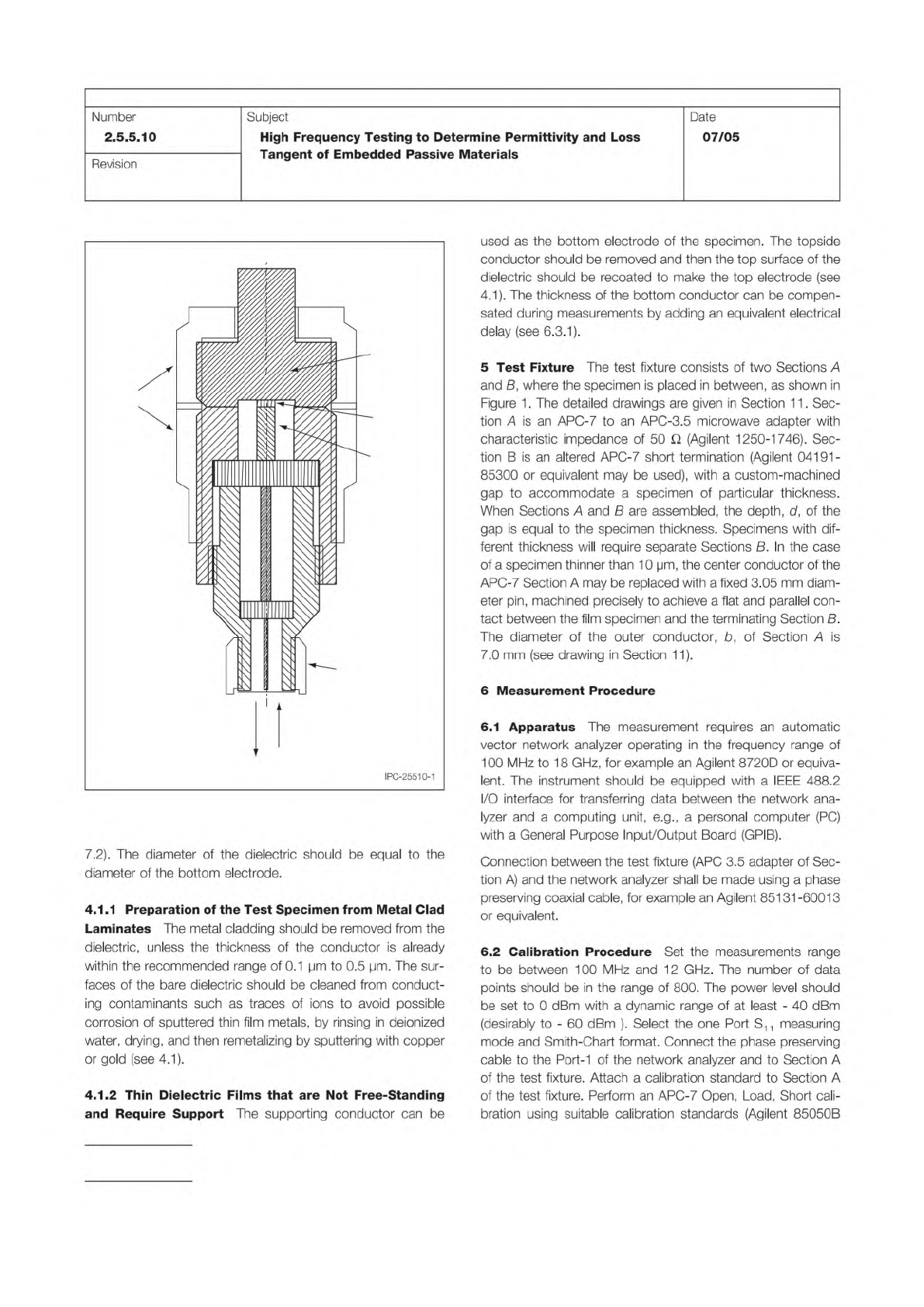
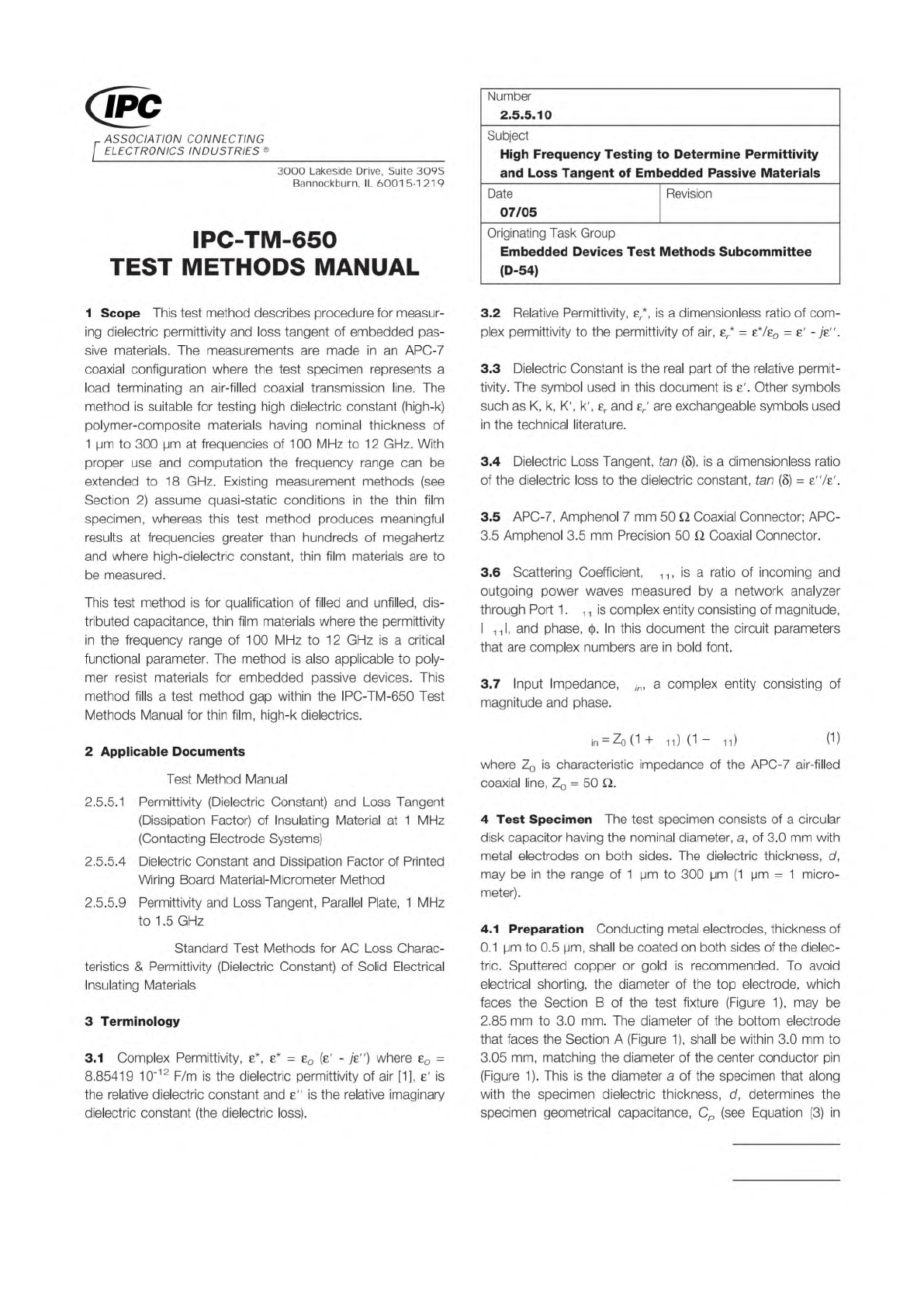
Figure 1 Test fixture with a test specimen between
Sections A and B
SECTION B
APC-7
Mount
SECTION A
APC-3.5 Port
to Network Analyzer, S
11
Short
Standard
with a Gap
Test
Specimen
Center
Conductor
Pin
IPC-TM-650
Page 2 of 8
Number
2.5.5.10
Revision
Subject
High
Frequency
Testing
to
Determine
Permittivity
and
Loss
Tangent
of
Embedded
Passive
Materials
Date
07/05
I
PC-2551
0-1
7.2).
The
diameter
of
the
dielectric
should
be
equal
to
the
diameter
of
the
bottom
electrode.
4.1.1
Preparation
of
the
Test
Specimen
from
Metal
Clad
Laminates
The
metal
cladding
should
be
removed
from
the
dielectric,
unless
the
thickness
of
the
conductor
is
already
within
the
recommended
range
of
0.1
pm
to
0.5
pm.
The
sur¬
faces
of
the
bare
dielectric
should
be
cleaned
from
conduct¬
ing
contaminants
such
as
traces
of
ions
to
avoid
possible
corrosion
of
sputtered
thin
film
metals,
by
rinsing
in
deionized
water,
drying,
and
then
remetalizing
by
sputtering
with
copper
or
gold
(see
4.1).
4.1.2
Thin
Dielectric
Films
that
are
Not
Free-Standing
and
Require
Support
The
supporting
conductor
can
be
used
as
the
bottom
electrode
of
the
specimen.
The
topside
conductor
should
be
removed
and
then
the
top
surface
of
the
dielectric
should
be
recoated
to
make
the
top
electrode
(see
4.1).
The
thickness
of
the
bottom
conductor
can
be
compen¬
sated
during
measurements
by
adding
an
equivalent
electrical
delay
(see
6.3.1).
5
Test
Fixture
The
test
fixture
consists
of
two
Sections
A
and
B,
where
the
specimen
is
placed
in
between,
as
shown
in
Figure
1
.
The
detailed
drawings
are
given
in
Section
1
1
.
Sec¬
tion
4
is
an
APC-7
to
an
APC-3.5
microwave
adapter
with
characteristic
impedance
of
50
Q
(Agilent
1250-1746).
Sec¬
tion
B
is
an
altered
APC-7
short
termination
(Agilent
04191-
85300
or
equivalent
may
be
used),
with
a
custom-machined
gap
to
accommodate
a
specimen
of
particular
thickness.
When
Sections
A
and
B
are
assembled,
the
depth,
d,
of
the
gap
is
equal
to
the
specimen
thickness.
Specimens
with
dif¬
ferent
thickness
will
require
separate
Sections
B.
In
the
case
of
a
specimen
thinner
than
1
0
pm,
the
center
conductor
of
the
APC-7
Section
A
may
be
replaced
with
a
fixed
3.05
mm
diam¬
eter
pin,
machined
precisely
to
achieve
a
flat
and
parallel
con¬
tact
between
the
film
specimen
and
the
terminating
Section
B.
The
diameter
of
the
outer
conductor,
b,
of
Section
A
is
7.0
mm
(see
drawing
in
Section
11).
6
Measurement
Procedure
6.1
Apparatus
The
measurement
requires
an
automatic
vector
network
analyzer
operating
in
the
frequency
range
of
100
MHz
to
1
8
GHz,
for
example
an
Agilent
8720D
or
equiva¬
lent.
The
instrument
should
be
equipped
with
a
IEEE
488.2
I/O
interface
for
transferring
data
between
the
network
ana¬
lyzer
and
a
computing
unit,
e.g.,
a
personal
computer
(PG)
with
a
General
Purpose
Input/Output
Board
(GP
旧).
Connection
between
the
test
fixture
(APO
3.5
adapter
of
Sec¬
tion
A)
and
the
network
analyzer
shall
be
made
using
a
phase
preserving
coaxial
cable,
for
example
an
Agilent
85131-60013
or
equivalent.
6.2
Calibration
Procedure
Set
the
measurements
range
to
be
between
100
MHz
and
12
GHz.
The
number
of
data
points
should
be
in
the
range
of
800.
The
power
level
should
be
set
to
0
dBm
with
a
dynamic
range
of
at
least
-
40
dBm
(desirably
to
-
60
dBm
).
Select
the
one
Port
S—
measuring
mode
and
Smith-Chart
format.
Connect
the
phase
preserving
cable
to
the
Port-1
of
the
network
analyzer
and
to
Section
A
of
the
test
fixture.
Attach
a
calibration
standard
to
Section
A
of
the
test
fixture.
Perform
an
APC-7
Open,
Load,
Short
cali¬
bration
using
suitable
calibration
standards
(Agilent
85050B
S
S S
Z
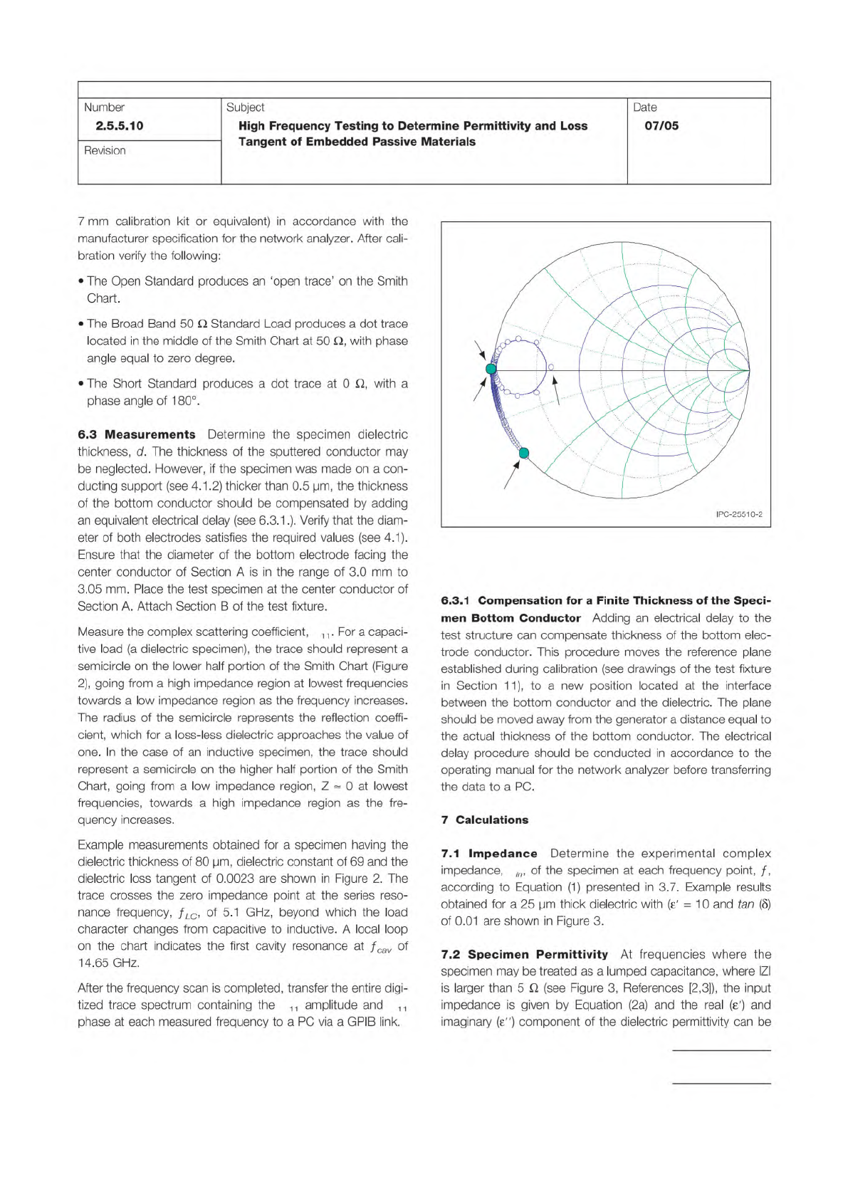
Figure 2 Example measurements plotted in a Smith chart
Format for an 80 µm thick specimen with permittivity of 69
- j0.16.
0.8 1.5 3.0 7.5
-0.8j
0.8j
-1.5j
1.5j
-3.0j
3.0j
-7.5j
7.5j
100 MHz
5.1 GHz
14.65 GHz
Z
in
~
0
~
IPC-TM-650
Page 3 of 8
Number
2.5.5.10
Subject
High
Frequency
Testing
to
Determine
Permittivity
and
Loss
Tangent
of
Embedded
Passive
Materials
Date
07/05
Revision
7
mm
calibration
kit
or
equivalent)
in
accordance
with
the
manufacturer
specification
for
the
network
analyzer.
After
cali¬
bration
verify
the
following:
•
The
Open
Standard
produces
an
'open
trace'
on
the
Smith
Chart.
•
The
Broad
Band
50
Q
Standard
Load
produces
a
dot
trace
located
in
the
middle
of
the
Smith
Chart
at
50
Q,
with
phase
angle
equal
to
zero
degree.
•
The
Short
Standard
produces
a
dot
trace
at
0
Q,
with
a
phase
angle
of
1
80°.
6.3
Measurements
Determine
the
specimen
dielectric
thickness,
d.
The
thickness
of
the
sputtered
conductor
may
be
neglected.
However,
if
the
specimen
was
made
on
a
con¬
ducting
support
(see
4.1.2)
thicker
than
0.5
pm,
the
thickness
of
the
bottom
conductor
should
be
compensated
by
adding
an
equivalent
electrical
delay
(see
6.3.
1.).
Verify
that
the
diam¬
eter
of
both
electrodes
satisfies
the
required
values
(see
4.1).
Ensure
that
the
diameter
of
the
bottom
electrode
facing
the
center
conductor
of
Section
A
is
in
the
range
of
3.0
mm
to
3.05
mm.
Place
the
test
specimen
at
the
center
conductor
of
Section
A.
Attach
Section
B
of
the
test
fixture.
Measure
the
complex
scattering
coefficient,
For
a
capaci¬
tive
load
(a
dielectric
specimen),
the
trace
should
represent
a
semicircle
on
the
lower
half
portion
of
the
Smith
Chart
(Figure
2),
going
from
a
high
impedance
region
at
lowest
frequencies
towards
a
low
impedance
region
as
the
frequency
increases.
The
radius
of
the
semicircle
represents
the
reflection
coeffi¬
cient,
which
for
a
loss-less
dielectric
approaches
the
value
of
one.
In
the
case
of
an
inductive
specimen,
the
trace
should
represent
a
semicircle
on
the
higher
half
portion
of
the
Smith
Chart,
going
from
a
low
impedance
region,
Z
«
0
at
lowest
frequencies,
towards
a
high
impedance
region
as
the
fre¬
quency
increases.
Example
measurements
obtained
for
a
specimen
having
the
dielectric
thickness
of
80
pm,
dielectric
constant
of
69
and
the
dielectric
loss
tangent
of
0.0023
are
shown
in
Figure
2.
The
trace
crosses
the
zero
impedance
point
at
the
series
reso¬
nance
frequency,
fLC,
of
5.1
GHz,
beyond
which
the
load
character
changes
from
capacitive
to
inductive.
A
local
loop
on
the
chart
indicates
the
first
cavity
resonance
at
/cav
of
14.65
GH
乙
After
the
frequency
scan
is
completed,
transfer
the
entire
digi¬
tized
trace
spectrum
containing
the
amplitude
and
口
phase
at
each
measured
frequency
to
a
PC
via
a
GPIB
link.
6.3.1
Compensation
for
a
Finite
Thickness
of
the
Speci¬
men
Bottom
Conductor
Adding
an
electrical
delay
to
the
test
structure
can
compensate
thickness
of
the
bottom
elec¬
trode
conductor.
This
procedure
moves
the
reference
plane
established
during
calibration
(see
drawings
of
the
test
fixture
in
Section
11),
to
a
new
position
located
at
the
interface
between
the
bottom
conductor
and
the
dielectric.
The
plane
should
be
moved
away
from
the
generator
a
distance
equal
to
the
actual
thickness
of
the
bottom
conductor.
The
electrical
delay
procedure
should
be
conducted
in
accordance
to
the
operating
manual
for
the
network
analyzer
before
transferring
the
data
to
a
PC.
7
Calculations
7.1
Impedance
Determine
the
experimental
complex
impedance,
in,
of
the
specimen
at
each
frequency
point,
/,
according
to
Equation
(1)
presented
in
3.7.
Example
results
obtained
for
a
25
pm
thick
dielectric
with
(o'
=
1
0
and
tan
(5)
of
0.01
are
shown
in
Figure
3.
7.2
Specimen
Permittivity
At
frequencies
where
the
specimen
may
be
treated
as
a
lumped
capacitance,
where
IZI
is
larger
than
5
Q
(see
Figure
3,
References
[2,3]),
the
input
impedance
is
given
by
Equation
(2a)
and
the
real
and
imaginary
(£〃)
component
of
the
dielectric
permittivity
can
be