IPC-TM-650 EN 2022 试验方法--.pdf - 第603页
[ [ [ Note: IPC-TM-650 Number Subject Date Revision Page 2 of 3 2.5.17.2 Volume Resistivity of Conductive Materials Used in High Density Interconnection (HDI) and Microvias, Two-Wire Method 11/98 3.1 Conductor Any high r…
[
[
IPC-TM-650
[
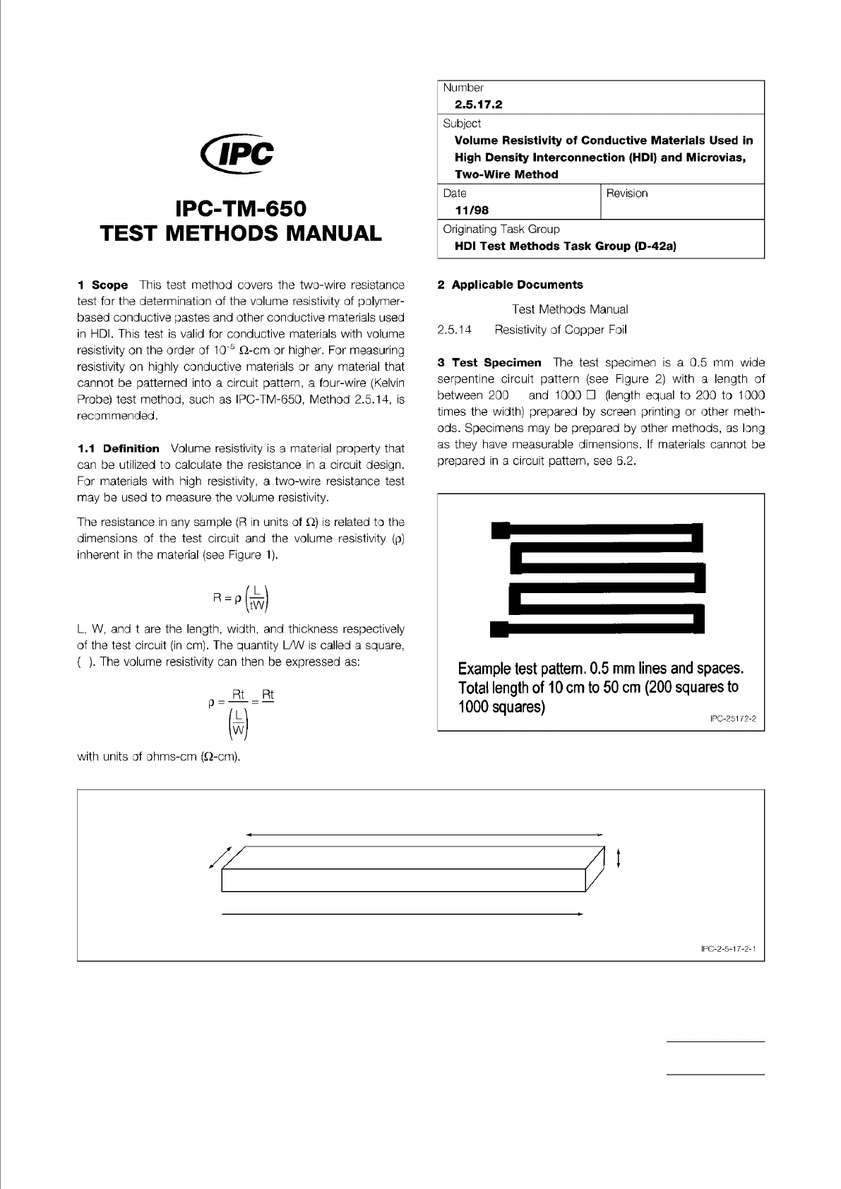
Figure 1 Resistivity Diagram
Conductor
Length = L
Current Flow
Width = W
Thickness = t
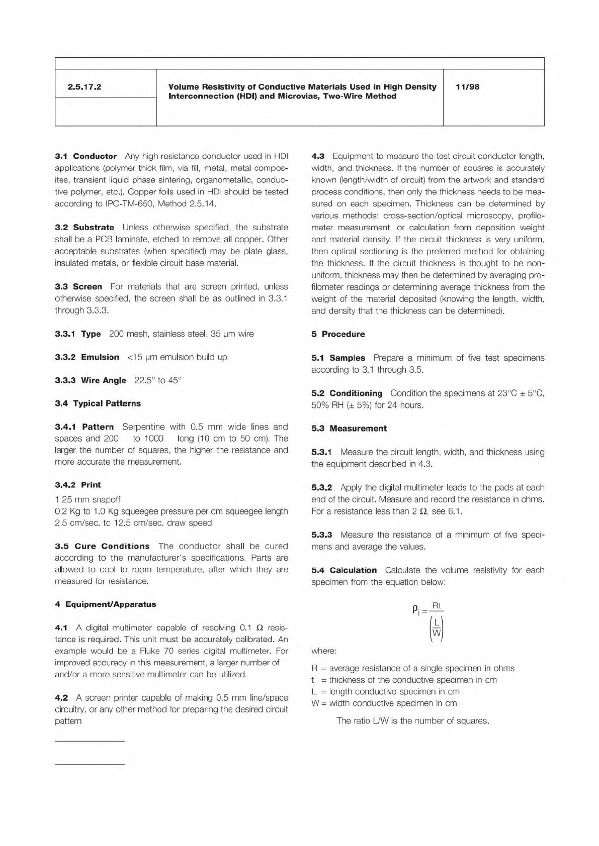
Figure 2 Serpentine Pattern
The Institute for Interconnecting and Packaging Electronic Circuits
2215 Sanders Road • Northbrook, IL 60062
Material in this Test Methods Manual was voluntarily established by Technical Committees of the IPC. This material is advisory only
and its use or adaptation is entirely voluntary. IPC disclaims all liability of any kind as to the use, application, or adaptation of this
material. Users are also wholly responsible for protecting themselves against all claims or liabilities for patent infringement.
Equipment referenced is for the convenience of the user and does not imply endorsement by the IPC.
Page 1 of 3
Number
回
IPC-TM-650
TEST
METHODS
MANUAL
1
Scope
This
test
method
covers
the
two-wire
resistance
test
for
the
determination
of
the
volume
resistivity
of
polymer¬
based
conductive
pastes
and
other
conductive
materials
used
in
HDI.
This
test
is
valid
for
conductive
materials
with
volume
resistivity
on
the
order
of
10-5
Q-cm
or
higher.
For
measuring
resistivity
on
highly
conductive
materials
or
any
material
that
cannot
be
patterned
into
a
circuit
pattern,
a
four-wire
(Kelvin
Probe)
test
method,
such
as
IPC-TM-650,
Method
2.5.14,
is
recommended.
1.1
Definition
Volume
resistivity
is
a
material
property
that
can
be
utilized
to
calculate
the
resistance
in
a
circuit
design.
For
materials
with
high
resistivity,
a
two-wire
resistance
test
may
be
used
to
measure
the
volume
resistivity.
The
resistance
in
any
sample
(R
in
units
of
Q)
is
related
to
the
dimensions
of
the
test
circuit
and
the
volume
resistivity
(p)
inherent
in
the
material
(see
Figure
1).
R
=
p
信)
L,
W,
and
t
are
the
length,
width,
and
thickness
respectively
of
the
test
circuit
(in
cm).
The
quantity
L/W
is
called
a
square,
(
).
The
volume
resistivity
can
then
be
expressed
as:
Rt Rt
p
=
—
=—
向
with
units
of
ohms-cm
(Q-cm).
2.5.17.2
Subject
Volume
Resistivity
of
Conductive
Materials
Used
in
High
Density
Interconnection
(HDI)
and
Microvias,
Two-
Wire
Method
Date
11/98
Revision
Originating
Task
Group
HDI
Test
Methods
Task
Group
(D-42a)
2
Applicable
Documents
Test
Methods
Manual
2.5.14
Resistivity
of
Copper
Foil
3
Test
Specimen
The
test
specimen
is
a
0.5
mm
wide
serpentine
circuit
pattern
(see
Figure
2)
with
a
length
of
between
200
and
1000
口
(length
equal
to
200
to
1000
times
the
width)
prepared
by
screen
printing
or
other
meth¬
ods.
Specimens
may
be
prepared
by
other
methods,
as
long
as
they
have
measurable
dimensions.
If
materials
cannot
be
prepared
in
a
circuit
pattern,
see
6.2.
IPC-2-5-1
7-2-1
[ [
[
Note:
IPC-TM-650
Number
Subject Date
Revision
Page 2 of 3
2.5.17.2
Volume
Resistivity
of
Conductive
Materials
Used
in
High
Density
Interconnection
(HDI)
and
Microvias,
Two-Wire
Method
11/98
3.1
Conductor
Any
high
resistance
conductor
used
in
HDI
applications
(polymer
thick
film,
via
fill,
metal,
metal
compos¬
ites,
transient
liquid
phase
sintering,
organometallic,
conduc¬
tive
polymer,
etc.).
Copper
foils
used
in
HDI
should
be
tested
according
to
IPC-TM-650,
Method
2.5.14.
3.2
Substrate
Unless
otherwise
specified,
the
substrate
shall
be
a
PCB
laminate,
etched
to
remove
all
copper.
Other
acceptable
substrates
(when
specified)
may
be
plate
glass,
insulated
metals,
or
flexible
circuit
base
material.
3.3
Screen
For
materials
that
are
screen
printed,
unless
otherwise
specified,
the
screen
shall
be
as
outlined
in
3.3.1
through
3.3.3.
3.3.1
Type
200
mesh,
stainless
steel,
35
pm
wire
3.3.2
Emulsion
<15
pm
emulsion
build
up
3.3.3
Wire
Angle
22.5°
to
45°
3.4
Typical
Patterns
3.4.1
Pattern
Serpentine
with
0.5
mm
wide
lines
and
spaces
and
200
to
1000
long
(10
cm
to
50
cm).
The
larger
the
number
of
squares,
the
higher
the
resistance
and
more
accurate
the
measurement.
3.4.2
Print
1
.25
mm
snapoff
0.2
Kg
to
1
.0
Kg
squeegee
pressure
per
cm
squeegee
length
2.5
cm/sec.
to
12.5
cm/sec.
draw
speed
3.5
Cure
Conditions
The
conductor
shall
be
cured
according
to
the
manufacturer's
specifications.
Parts
are
allowed
to
cool
to
room
temperature,
after
which
they
are
measured
for
resistance.
4
Equipment/Apparatus
4.1
A
digital
multimeter
capable
of
resolving
0.1
Q
resis¬
tance
is
required.
This
unit
must
be
accurately
calibrated.
An
example
would
be
a
Fluke
70
series
digital
multimeter.
For
improved
accuracy
in
this
measurement,
a
larger
number
of
and/or
a
more
sensitive
multimeter
can
be
utilized.
4.2
A
screen
printer
capable
of
making
0.5
mm
line/space
circuitry,
or
any
other
method
for
preparing
the
desired
circuit
pattern
4.3
Equipment
to
measure
the
test
circuit
conductor
length,
width,
and
thickness.
If
the
number
of
squares
is
accurately
known
(length/width
of
circuit)
from
the
artwork
and
standard
process
conditions,
then
only
the
thickness
needs
to
be
mea¬
sured
on
each
specimen.
Thickness
can
be
determined
by
various
methods:
cross-section/optical
microscopy,
profilo¬
meter
measurement,
or
calculation
from
deposition
weight
and
material
density.
If
the
circuit
thickness
is
very
uniform,
then
optical
sectioning
is
the
preferred
method
for
obtaining
the
thickness.
If
the
circuit
thickness
is
thought
to
be
non-
uniform,
thickness
may
then
be
determined
by
averaging
pro¬
filometer
readings
or
determining
average
thickness
from
the
weight
of
the
material
deposited
(knowing
the
length,
width,
and
density
that
the
thickness
can
be
determined).
5
Procedure
5.1
Samples
Prepare
a
minimum
of
five
test
specimens
according
to
3.1
through
3.5.
5.2
Conditioning
Condition
the
specimens
at
23℃
土
5
℃,
50%
RH
(±
5%)
for
24
hours.
5.3
Measurement
5.3.1
Measure
the
circuit
length,
width,
and
thickness
using
the
equipment
described
in
4.3.
5.3.2
Apply
the
digital
multimeter
leads
to
the
pads
at
each
end
of
the
circuit.
Measure
and
record
the
resistance
in
ohms.
For
a
resistance
less
than
2
Q,
see
6.1.
5.3.3
Measure
the
resistance
of
a
minimum
of
five
speci¬
mens
and
average
the
values.
5.4
Calculation
Calculate
the
volume
resistivity
for
each
specimen
from
the
equation
below:
where:
R
=
average
resistance
of
a
single
specimen
in
ohms
t
二
thickness
of
the
conductive
specimen
in
cm
L
=
length
conductive
specimen
in
cm
W
=
width
conductive
specimen
in
cm
The
ratio
L/W
is
the
number
of
squares.
photolithographic processes such that a minimum of twelve
good specimens are yielded at the end of 3.4.5. On the ‘‘Test
Surface,’’ etch four conductors 3.2 mm [0.126 in] wide,
5.7 mm [0.224 in] pitch, 230 - 250 mm [9 - 10 in] long on a
nominal 25 mm [1 in] wide strip of flexible base dielectric (see
Figures 1 and 2).
3.4 Conditioning and Aging Procedure
3.4.1
Twelve specimens, as described in section 3, be
subjected to a stabilization period of a minimum of 24 hours
at 23 °C ± 2 °C [73.4 °F ± 3.6 °F] and 50% ± 5% RH.
IPC-2-6-21a
Metal Conductor (4 each)
3.2 mm
[0.126 in]
25 mm [1 in]
(nom.)
230–250 mm [9–10 in]
5.7 mm
[0.224 in]
1 Soak Clean
Use commercially available acid or alkaline
cleaners
Per supplier recommended
temperature
Per supplier recommended
time
2 Rinse Running tap water Room Temperature 3 - 5 minutes
3 Microetch
Sodium persulfate: Two liters of deionized
water, 280 grams of sodium persulfate,
25 cc sulfuric acid
Room Temperature 1 - 2 minutes
4 Rinse Running tap water Room Temperature 1 minute
5 Acid Dip
Sulfuric acid 10% by volume, dilution 1.8
liters deionized water, 200 cc sulfuric acid
96% assay
Room Temperature 45 seconds
6 Rinse Running tap water Room Temperature 1 minute
7 Rinse Deionized water Room Temperature 1 minute
8 Dry Force air dry or blot with paper towels Room Temperature 1 - 3 minutes
9 Bake Bake in clean air-circulating oven 110 ± 5 °C [230.0 ± 9.0 °F] 10 to 15 minutes
10 Lamination
*Maximum delay between bake and
lamination
be 30 minutes
*Lamination conditions (e.g., pressure, temperature, time, etc.) conform to suppliers’ recommendations.
Number
2.6.21
Subject
Service Temperature of Metal-Clad Flexible Laminate, Cover
Material and Adhesive Bonding Films
Date
6/11
Revision
B
IPC-TM-650
—
Figure
1
Construction
of
Specimens
for
Peel
Strength
Testing
Table
1
Cleaning
Process
for
Shiny
Copper
shall
Step
Process
Material
Temperature
Time
shall
shall
Page
2
of
5