IPC-TM-650 EN 2022 试验方法--.pdf - 第507页
Figure 1 Distance from Clips The Institute for Int erconnecting and Packaging E lectronic Circuits 2215 Sanders Road • Northbrook, IL 60062 Material in this T est M ethods Manual was voluntarily establis hed by T echni c…

assumption invalid and introduces errors in the reported
delay
b. Short test lines reducing the t
D
accuracy due to system
temporal limits (see 4.1.2)
c. Short test lines reducing ability to identify intentional dis-
continuities from signal launch
d. Long test lines detrimentally reducing amplitude of reflec-
tion signal due to large skin effect and dielectric losses
2 Applicable Documents
Design Guide for High-Speed Controlled Imped-
ance Circuit Boards
Test Methods Manual
1.9 Measurement Precision Estimation for Variables Data
2.5.5.7 Characteristic Impedance of Lines on Printed Boards
by TDR
3 Test Specimens
The test specimen can take one of sev-
eral forms depending on the application, but it must contain at
least one transmission line (or interconnect) test structure and
be representative of the actual PB product. Four definite types
of specimens are described in 3.1.1 through 3.1.4. The trans-
mission lines to be measured may be of either stripline or
microstrip construction.
3.1 Test Specimen Examples
3.1.1 Example 1
Test specimens are representative PBs
selected out of a lot of fabricated product. In some cases, this
sample set may contain all PBs in the lot. Agreed upon func-
tional and nonfunctional transmission lines on the PB are used
as the test set for this specimen. The selection of lines that
form the test set must be based on these criteria (nonexclu-
sive):
a. Inclusion of the PB’s critical features
b. Accessible line terminations for measurements
c. Absence of line branching
d. Absence of impedance changes within the transmission
line under test
e. Representation of controlled characteristic impedance Z
0
signal layers
3.1.2 Example 2
Test specimens are representative fabri-
cated PB samples or entire lots as in 3.1.1. The test lines used
in these specimens are nonfunctional lines designed into the
PB for easy termination and connection to TDR equipment.
Such test lines should be designed to include critical features
typical of functional lines and should lie in the controlled Z
0
signal layers of the application.
3.1.3 Example 3
Test specimens are test coupons cut
from representative fabricated PB samples or entire lots. The
test coupons are cut from the master PB at the time the indi-
vidual PBs are separated. Such test coupons will have one or
more nonfunctional transmission lines with termination suited
for TDR testing. Such test lines should include critical features
typical of functional lines and will be fabricated in the same
configuration and structure as the master PB on the same
controlled Z
0
signal layers as the application.
3.1.4 Example 4
Test specimens are a sample of the sub-
strate laminate to be characterized before PB manufacturing
and fabrication. The test line fabrication on these specimens
may involve laminating several PB layers together in the same
manner anticipated for PB manufacture.
3.2 Identification of Test Specimen
For specimens of
types called out in 3.1.1, 3.1.2, or 3.1.3, each specimen
be identified with no less than a PB part number, PB serial
number, and date code. Specimens of the type called for in
3.1.4 must include the lot or panel identification for the sub-
strate laminate being evaluated.
3.3 Conditioning
Environmental conditioning prior to test
may be called for as part of the test. When conditioning is
required, test specimens
be stored before testing at 23
+1/-5 °C and 50 ± 5% RH for no less than 16 hours. If a dif-
ferent conditioning procedure is required, it must be specified
and documented in test reports.
3.4 Test Interconnect Placement
The ability to correlate
propagation delay values derived from measurements of non-
functional test lines to propagation delay values of functional
lines is directly related to the proximity of the nonfunctional
test structure to the functional lines. The closer the test and
functional lines, the more likely the nominal material properties
will be the same. The placement of test structures on the PB
or panel should be analyzed for each PB design and be based
on the propagation delay tolerance and practicality of the lay-
out. When deciding on the best test interconnect placement,
consider the following placement priorities:
1) Inside the functional area of the PB;
2) At the edge of the PB but outside the functional circuit
area; or
Number
2.5.5.11
Subject
Propagation Delay of Lines on Printed Boards by TDR
Date
04/2009
Revision
IPC-TM-650
IPC-2141
IPC-TM-650
shall
Page
2
of
16
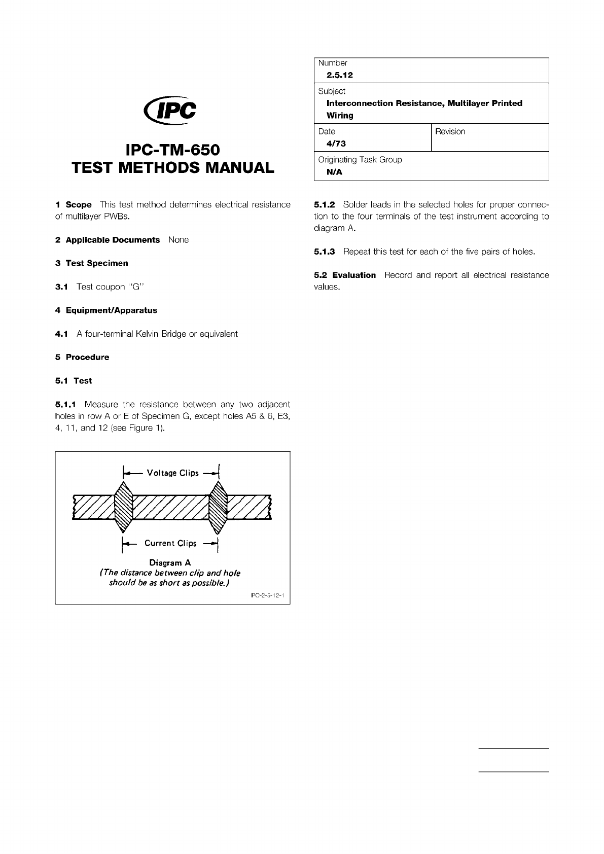
Figure 1 Distance from Clips
The Institute for Interconnecting and Packaging Electronic Circuits
2215 Sanders Road • Northbrook, IL 60062
Material in this Test Methods Manual was voluntarily established by Technical Committees of the IPC. This material is advisory only
and its use or adaptation is entirely voluntary. IPC disclaims all liability of any kind as to the use, application, or adaptation of this
material. Users are also wholly responsible for protecting themselves against all claims or liabilities for patent infringement.
Equipment referenced is for the convenience of the user and does not imply endorsement by the IPC.
Page 1 of 1
回
IPC-TM-650
TEST
METHODS
MANUAL
1
Scope
This
test
method
determines
electrical
resistance
of
multilayer
PWBs.
2
Applicable
Documents
None
3
Test
Specimen
3.1
Test
coupon
"G”
4
Equipment/Apparatus
4.1
A
four-terminal
Kelvin
Bridge
or
equivalent
5
Procedure
5.1
Test
5.1.1
Measure
the
resistance
between
any
two
adjacent
holes
in
row
A
or
E
of
Specimen
G,
except
holes
A5
&
6,
E3,
4,
11
,
and
12
(see
Figure
1).
Diagram
A
(The
distance
between
dip
and
hole
should
be
as
short
as
possible.)
Number
2.5.12
Subject
Interconnection
Resistance,
Multilayer
Printed
Wiring
Date
Revision
4/73
Originating
Task
Group
N/A
5.1.2
Solder
leads
in
the
selected
holes
for
proper
connec¬
tion
to
the
four
terminals
of
the
test
instrument
according
to
diagram
A.
5.1.3
Repeat
this
test
for
each
of
the
five
pairs
of
holes.
5.2
Evaluation
Record
and
report
all
electrical
resistance
values.
I
PC-2-5-1
2-1
interconnects, but a practical issue of operator ability to use
hand-held probes may be considered. Test reports must
report any deviation from the nominal contact land and PTH
geometry.
3.9 Contact Land Pitch
Whenever possible, the center-
to-center distance between the signal and reference lands
of the test interconnect should be consistent to simplify
probing requirements and ensure measurement repeatability
and reproducibility. Nominal center-to-center pitch
be
1.91 mm [0.075 in]. The use of different contact and probe
pitches must be specified and documented.
3.10 Single-Signal Conductor Transmission Line
The
single-signal conductor transmission line is also known as the
single-ended, unbalanced, and asymmetrical structure. The
probing area for these lines should consist of a contact land
(see Figure 3-2) for each signal line. The contact land should
provide connection to the reference, or ground, connection for
the test structure. This method requires the use of one con-
tact pitch to ensure measurement consistency between the
test structures of the specimen.
3.11 Orientation
The contact land orientation (placement
and angle of the contact land of the signal line relative to the
contact land of the reference plane) must be the same for all
test interconnects of the specimen in order to ensure mea-
surement consistency between test interconnects.
3.12 Test Interconnect Routing
a. The test interconnects only be routed over and under
contiguous ground and voltage planes following controlled
line impedance guidelines (see IPC-2141). The test inter-
connects must not extend into PTH clearance areas.
b. The test interconnects
be kept at least six times the
width of the signal conductor or 2.5 mm [0.0984 in],
whichever is greater, from any PTHs and any other inter-
connect on the same plane. All conductive material (such
as copper nomenclature, copper thieving, etc.)
be
kept at least 2.5 mm [0.0984 in] from each test intercon-
nect.
c. Test interconnects
be straight or contain gradual and
rounded bends.
3.13 Nomenclature
Labeling of all test interconnect con-
tact lands on at least one surface layer is required for opera-
tor identification during manual probing operations. The label
minimally contain information about which signal layer
the test interconnect is modeling (for example, L1-3in, L1-6in,
etc.). Nomenclature should be etched in copper and be
spaced a minimum of at least six times the width of the signal
conductor (of the test interconnect) or 2.5 mm [0.0984 in],
whichever is greater, from the test interconnect area. When-
ever practical, the terminations at both ends of test intercon-
nect
be marked.
IPC-25511-3-2
Number
2.5.5.11
Subject
Propagation Delay of Lines on Printed Boards by TDR
Date
04/2009
Revision
IPC-TM-650
shall
shall
shall
shall
shall
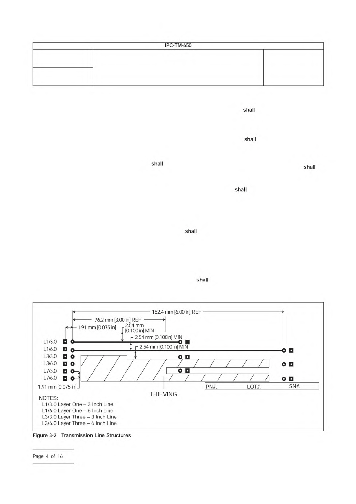
152.4
mm
[6.00
in]
REF
76.2
mm
[3.00
in]
REF
1.91
mm
[0.075
in]
厂
2.54
mm
[0.100
in]
MIN
2
口
/ /
/
/
/
SN#.
1.91
mm
[0.075
in]-
PN#.
LOT#.
L1/3.0
L1/6.0
L3/3.0
L3/6.0
L7/3.0
L7/6.0
2.54
mm
[0.100
in]
MIN
2.54
mm
[O.IOOin]
MIN
NOTES:
L1/3.0
Layer
One
-
3
Inch
Line
L1/6.0
Layer
One
-
6
Inch
Line
L3/3.0
Layer
Three
-
3
Inch
Line
L3/6.0
Layer
Three
-
6
Inch
Line
THIEVING
Figure
3-2
Transmission
Line
Structures
Page
4
of
16