IPC-TM-650 EN 2022 试验方法--.pdf - 第591页
The Institute for Int erconnecting and Packaging E lectronic Circuits 2215 Sanders Road • Northbrook, IL 60062 Material in this T est M ethods Manual was voluntarily establis hed by T echni cal Committees of the IP C. Th…
IPC-B-25
IPC-B-25A
IPC-6012A
IPC-9201
ASTM D-257-93
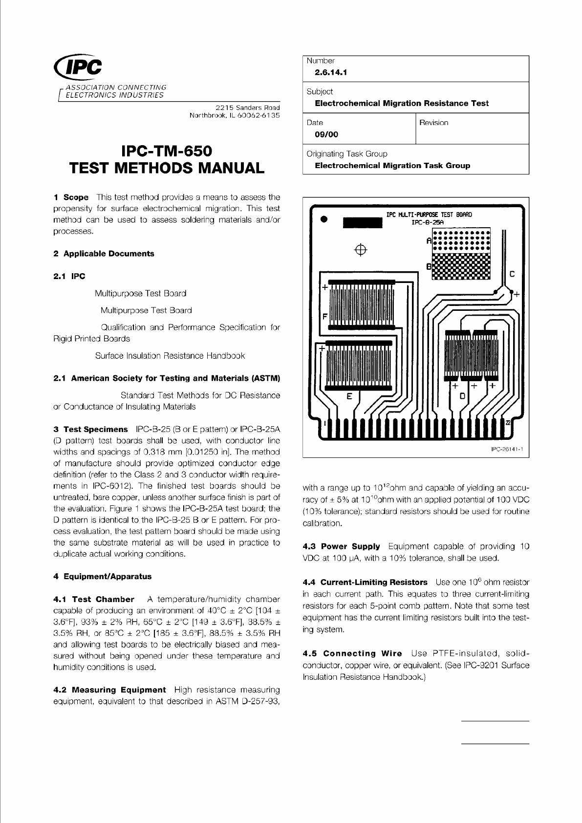
Figure 1 IPC-B-25A Test Board
Material in this Test Methods Manual was voluntarily established by Technical Committees of IPC. This material is advisory only
and its use or adaptation is entirely voluntary. IPC disclaims all liability of any kind as to the use, application, or adaptation of this
material. Users are also wholly responsible for protecting themselves against all claims or liabilities for patent infringement.
Equipment referenced is for the convenience of the user and does not imply endorsement by IPC.
Page 1 of 3
ASSOCIATION
CONNECTING
/
ELECTRONICS
INDUSTRIES
221
5
Sanders
Road
Northbrook,
IL
60062-61
35
IPC-TM-650
TEST
METHODS
MANUAL
1
Scope
This
test
method
provides
a
means
to
assess
the
propensity
for
surface
electrochemical
migration.
This
test
method
can
be
used
to
assess
soldering
materials
and/or
processes.
2
Applicable
Documents
2.1
IRC
Multipurpose
Test
Board
Multipurpose
Test
Board
Qualification
and
Performance
Specification
for
Rigid
Printed
Boards
Surface
Insulation
Resistance
Handbook
2.1
American
Society
for
Testing
and
Materials
(ASTM)
Standard
Test
Methods
for
DC
Resistance
or
Conductance
of
Insulating
Materials
3
Test
Specimens
IPC-B-25
(B
or
E
pattern)
or
IPC-B-25A
(D
pattern)
test
boards
shall
be
used,
with
conductor
line
widths
and
spacings
of
0.318
mm
[0.01250
in].
The
method
of
manufacture
should
provide
optimized
conductor
edge
definition
(refer
to
the
Class
2
and
3
conductor
width
require¬
ments
in
IPC-601
2).
The
finished
test
boards
should
be
untreated,
bare
copper,
unless
another
surface
finish
is
part
of
the
evaluation.
Figure
1
shows
the
IPC-B-25A
test
board;
the
D
pattern
is
identical
to
the
IPG-B-25
B
or
E
pattern.
For
pro¬
cess
evaluation,
the
test
pattern
board
should
be
made
using
the
same
substrate
material
as
will
be
used
in
practice
to
duplicate
actual
working
conditions.
4
Equipment/Apparatus
4.1
Test
Chamber
A
temperature/humidity
chamber
capable
of
producing
an
environment
of
40℃
±
2
℃
[104
±
36F],
93%
土
2%
RH,
65℃
±
2
℃
[149
±
3.6°F],
88.5%
±
3.5%
RH,
or
85℃
+
2
℃
[185
土
3.6°F],
88.5%
土
3.5%
RH
and
allowing
test
boards
to
be
electrically
biased
and
mea¬
sured
without
being
opened
under
these
temperature
and
humidity
conditions
is
used.
Number
2.6.14.1
Subject
Electrochemical
Migration
Resistance
Test
Date
Revision
09/00
Originating
Task
Group
Electrochemical
Migration
Task
Group
IPG-261
41-1
with
a
range
up
to
1012ohm
and
capable
of
yielding
an
accu¬
racy
of
+
5%
at
101°ohm
with
an
applied
potential
of
100
VDC
(10%
tolerance);
standard
resistors
should
be
used
for
routine
calibration.
4.3
Power
Supply
Equipment
capable
of
providing
10
VDC
at
100
pA,
with
a
10%
tolerance,
shall
be
used.
4.4
Current-Limiting
Resistors
Use
one
1
03
6
ohm
resistor
in
each
current
path.
This
equates
to
three
current-limiting
resistors
for
each
5-point
comb
pattern.
Note
that
some
test
equipment
has
the
current
limiting
resistors
built
into
the
test¬
ing
system.
4.5
Connecting
Wire
Use
PTFE-insulated,
solid¬
conductor,
copper
wire,
or
equivalent.
(See
IPC-9201
Surface
Insulation
Resistance
Handbook.)
4.2
Measuring
Equipment
High
resistance
measuring
equipment,
equivalent
to
that
described
in
ASTM
D-257-93,
The Institute for Interconnecting and Packaging Electronic Circuits
2215 Sanders Road • Northbrook, IL 60062
Material in this Test Methods Manual was voluntarily established by Technical Committees of the IPC. This material is advisory only
and its use or adaptation is entirely voluntary. IPC disclaims all liability of any kind as to the use, application, or adaptation of this
material. Users are also wholly responsible for protecting themselves against all claims or liabilities for patent infringement.
Equipment referenced is for the convenience of the user and does not imply endorsement by the IPC.
Page 1 of 5
IPC-TM-650
TEST
METHODS
MANUAL
1
Scope
It
is
the
intent
of
these
guidelines
to
describe
the
material
properties
and
test
procedures
required
to
ensure
effective
RFI
and
EMI
shielding
of
flat
cable.
1.2
Definitions
1.2.1
Relative
Shielding
Effectiveness
The
attenuation
difference
in
the
electromagnetic
field
strength
between
an
unprotected
cable
and
a
shielded
cable
system,
which
is
expressed,
S
=
Rx
+
A
+
B,
where:
Rx
二
the
losses
caused
by
reflection
in
db
A
=
the
losses
caused
by
absorption
in
db
B
二
the
secondary
reflection
losses
of
the
shields
in
db.
The
reflection
losses
are
a
function
of
the
material,
frequency,
and
type
of
field.
Generally,
the
field
within
one
wave
length
from
a
generating
source
will
either
be
predominantly
electric
or
magnetic,
and
at
greater
distance
will
propagate
as
a
plane
wave
made
up
equally
of
electric
and
magnetic
components.
Thus,
the
reflection
losses
for
each
of
these
fields
may
be
designated
by:
Re
=
electric
or
“E”
field
Rh
二
magnetic
or
''H''
field
Rp
=
plane
wave
field
The
absorption
losses
are
a
function
of
the
material
and
fre¬
quency
but
are
independent
of
field
type.
If
these
losses
(A)
are
greater
than
10
db,
the
secondary
reflection
losses
are
negligible,
and
the
expression
for
shielding
effectiveness
reduces
to
S
=
R
+
A.
The
following
are
standard
equations
that
may
be
used
to
obtain
a
rough
approximation
of
a
shield's
effectiveness.
Absorption
Losses:
A
=
3.38
X
10-3t
(uGf)i/2
Reflection
losses:
1
.
Plane
wave
Rp
=
108.2
+
10
log
2.
Magnetic
fields
RH
=
20
log
(蒋)
正
+0.136
r
(梨)
於
+
0.354
(r
<X)
Number
2.5.15
Subject
Guidelines
and
Test
Methods
for
RFI-EMI
Shielding
of
Flat
Cable
Date
Revision
10/86
A
Originating
Task
Group
N/A
3.
Electric
fields
Re
=
353.6
+
10
log
鸟
urr
(r
4)
where:
G
=
conductivity
relative
to
copper
u
=
magnetic
permeability
relative
to
free
space
f
=
frequency
in
Hertz
r
=
distance
from
source
to
shield
in
2.5
cm
t
二
thickness
of
metal
shield
in
0.0025
mm
九
=
wavelength
A
field
surrounds
every
source
of
electric
energy.
The
simple
situation
of
an
electric
current
flowing
through
a
wire
causes
a
field
to
exist
around
the
wire,
whose
magnitude
and
direction
follow
well-known
principles.
Part
of
the
energy
in
any
field
is
propagated
through
space
and
eventually
dampens
to
zero.
The
remaining
part
of
the
energy
of
a
field
either
returns
to
its
origin
or
is
absorbed
by
some
receiving
source.
A
dipole
antenna
behaves
in
this
manner;
part
of
its
energy
becomes
a
radiation
field,
while
another
portion
(that
periodically
returns
to
the
antenna)
becomes
the
induction
field.
The
general
mathematical
expression
that
describes
an
electromagnetic
field
is
rather
complex
and
is
usually
discussed
in
texts
on
field
theory.
It
is
easier
to
discuss
this
expression
in
terms
of
its
electric
vector
E
and
its
magnetic
vector
B,
where
E
has
the
dimension
of
V/1
and
units
of
volt/meter
and
B
has
the
dimen¬
sions
of
W12
and
units
of
volt-second/meter2
.
E
and
B
can
then
be
written
as
the
sum
of
two
components:
E
=
Ej
+
Er
B
=
Bj
+
Br
The
components
of
the
induction
field
are
E,
and
B,,
while
the
components
of
the
radiation
field
are
given
as
ER
and
BR,
ER,
and
Br
are
proportional
to
Bo/R
(Bo
=
w/voR,
where
w
is
the
angular
frequency
of
the
field
in
radians
and
vo
is
the
velocity
of
propagation
in
meters
per
second.)
E
)
and
B
)
are
propor¬
tional
to
1/R2,
where
R
is
the
distance
from
the
source
in
meters.
The
ratio
of
the
two
is
BOR
or
wR/vo.
It
can
be
con¬
cluded
from
this
that
for
very
small
values
of
R
and
any
given
values
for
w
and
vo,
the
induction
field
will
be
so
much
greater
than
the
radiation
field,
that
the
latter
may
be
neglected.
How¬
ever,
if
R
is
very
large,
the
radiation
field
is
important
and
the
induction
field
can
be
discarded.
IPC-TM-650
Number
Subject Date
Revision
Page 2 of 5
2.5.15
Guidelines
and
Test
Methods
for
RFI-EMI
Shielding
of
Flat
Cable
10/86
A
Induction
fields
are
either
high-
or
low-impedance
fields.
A
high-impedance
field
is
defined
as
a
field
whose
impedance
is
higher
than
the
impedance
of
the
dielectric
in
which
it
exists.
A
low-impedance
field
has
an
impedance
lower
than
the
impedance
of
the
dielectric.
High-impedance
fields
are
asso¬
ciated
with
a
voltage
source
and
most
of
their
energy
is
con¬
tained
in
their
electric
component,
while
low-impedance
fields
are
associated
with
a
current
source
and
most
of
their
energy
is
contained
in
the
magnetic
component.
1.2.2
Shield
Impedance
An
important
parameter
associ¬
ated
with
these
radiating
fields
is
the
characteristic
imped¬
ance,
which
is
the
ratio
of
the
electric
to
magnetic
field
com¬
ponents.
For
a
plane
wave
in
free
space,
the
characteristic
impedance
is
377
ohms,
and
correspondingly
for
intense
electric
or
high
impedance
fields,
it
is
greater
than
377
ohms,
and
for
strong
magnetic
or
low
impedance
fields,
it
is
less
than
377
ohms.
The
difference
in
characteristic
impedance
between
an
incident
field
and
a
shield
is
directly
proportional
to
the
reflection
losses.
The
characteristic
impedance
of
a
shield
varies
with
the
material's
permeability,
conductivity,
and
frequency.
Shield
impedances
are
generally
low
at
low
fre¬
quencies
and
increase
directly
with
frequency.
Since
at
all
fre¬
quencies,
electric
(E)
fields
are
high
impedance
and
magnetic
(H)
fields
are
low
impedance,
the
corresponding
reflection
losses
are
high
for
electric
fields
at
low
test
frequency
and
low
or
poor
for
magnetic
fields
at
the
same
test
frequency.
As
test
frequencies
increase,
the
impedance
mismatches
decrease
for
electric
fields
(decrease
in
RE)
and
increase
for
magnetic
fields
(increase
in
RH).
The
absorption
losses
for
both
electric
and
magnetic
fields
increase
with
frequency.
It
can
be
con¬
cluded
from
this
that
good
shielding
effectiveness
against
pre¬
dominantly
electric
fields
can
be
obtained
with
most
high
con¬
ductivity
shielding
materials.
At
low
frequencies,
Re
losses
are
so
high
that
small
absorption
losses
may
be
neglected
and,
at
high
frequencies,
even
though
most
of
the
transmitted
energy
is
coupled
to
the
shield,
absorption
losses
are
high
enough
for
adequate
shielding
if
all
nonconductive
openings
in
the
shield
are
eliminated.
Shielding
against
magnetic
fields
presents
a
different
situation
at
low
frequencies,
where
absorption
and
reflection
(RH)
losses
are
small.
Here,
uniform
100%
shielding
is
essential
and
in
most
cases
ferromagnetic,
highly
perme¬
able
materials
are
employed
to
increase
absorption
losses.
At
high
frequencies,
both
reflection
and
absorption
losses
are
high,
and
shielding
effectiveness
is
good
for
magnetic
fields.
Table
1
shows
properties
of
various
metals
at
150
KHz
and
400
MHz
and
the
corresponding
absorption
loss
in
db.
The
significance
of
this
table
is
to
show
the
necessity
for
highly
permeable
materials
to
shield
against
low
frequency
magnetic
fields.
3
Test
Specimen
None
4
Equipment/Apparatus
None
5
Procedure
None
6
Notes
6.1
Shielding
effectiveness
is
usually
determined
more
pre¬
cisely
by
measurement
than
by
calculation,
especially
when
100%
shielding
is
impractical.
To
obtain
the
attenuation
capa¬
bility
of
a
shielding
material
about
a
flat
cable,
it
is
more
prac¬
tical
to
test
a
cable
system
for
its
susceptibility
to
radiated
energy.
Figure
1
shows
a
test
setup
designed
to
measure
shielding
effectiveness
in
a
flat
cable
for
electric
and
magnetic
radiating
fields.
Two
1
.5
m
cable
specimens,
one
shielded
and
one
unshielded,
are
terminated
in
their
characteristic
impedance
at
the
generator
source
end
and
attached
through
a
coaxial
switch
to
a
field
intensity
meter
(or
similar
device)
at
the
other
end.
These
two
cable
samples
are
mounted
and
suspended
2.5
cm
above
a
conducting
ground
plane
and
7.5
cm
to
either
side
of
a
bare
unshielded
copper
wire
(see
Figure
2).
This
radiating
copper
wire
is
connected
at
one
end
to
a
RF
signal
generator
and
is
terminated
at
the
opposite
end
in
either
a
short
or
non-radiating
open
circuit.
6.2
When
the
bare
wire
is
open
circuited,
the
majority
of
the
radiated
field
is
electric,
and
when
it
is
short
circuited,
mag¬
netic
fields
dominate.
Since
the
cables
are
only
7.5
cm
away
from
the
radiating
source,
electric
and
magnetic
shielding
effectiveness
can
be
measured
separately
at
frequencies
up
to
approximately
4
GHz.
It
is
assumed
that
if
a
shield
is
effec¬
tive
under
these
conditions,
it
will
be
equally
effective
against
plane
wave
radiation.
6.3
Four
readings
must
be
taken
at
each
test
frequency.
First
the
voltage
pick-up
in
the
unshielded
specimen
is
observed
and
is
used
as
the
reference
level
for
the
voltage
measurement
on
the
shielded
line.
The
shielding
effectiveness
in
decibels
is
given
by:
S
=
20
log
VUA/S
where:
Vu
=
voltage
induced
into
unshielded
cable
Vs
=
voltage
induced
into
shielded
cable