IPC-TM-650 EN 2022 试验方法--.pdf - 第563页
IPC-TM-650 Number S ubject Date Revision 4.5 Micrometer A micrometer with a minimal resolution of 0.001mm [0.00004 inch] or better. 4.6 Circulating Oven An air circulating oven with capable of a temperature of 105 ± 1 ° …

During the remainder of the preparation, handle boards by the
edges only and use noncontaminating gloves.
3.1.3
Dry the cleaned boards for two hours at 50 °C.
3.1.4
If boards are to be stored before treatment, place the
boards in Kapak™ bags or other contamination-free contain-
ers (do not heat seal) in a desiccator. (Kapak™ bags are avail-
able from Fischer, VWR and other distributors.)
3.1.5
When measured as described in Sections 4 and 5, if
the control board readings are less than 1000 MΩ at any point
after the initial 24 hours of SIR exposure, a new set of test
coupons shall be obtained and the entire test repeated.
3.2 Blank Process Controls
If performing process valida-
tion testing, two samples from an unprocessed blank should
be run with the samples taken from the processed boards.
Values obtained from unprocessed board samples are useful
when failure is observed within the processed board sample.
Failure of the unprocessed samples may indicate a problem
with the incoming bare board rather than an assembly pro-
cess.
4 Equipment/Apparatus
It is the responsibility of the user
of this method to verify equipment suitability. This method
intends for all tolerances to be interpreted as uncertainties
with a confidence interval of 95% as referenced in ANSI/NCSL
Z540-1 and ANSI/NCSL Z540-2. Quantitative, qualitative and
default information follow in the paragraphs below.
4.1 Electrometer
Electrometer, High Resistance Meter,
Picoammeter or equivalent as described by ASTM D 257.
a) System must be capable of taking measurements and
controlling the switching automatically (unattended).
b) Minimum resistance measurement accuracy (not only
meter, but as implemented)
5% of full scale up to 10
10
Ω @ 5V
10% of full scale up to 10
11
Ω @ 5V
20% of full scale above 10
11
Ω @ 5V
c) Accuracy with respect to the ‘‘true’’ value requires assess-
ment of stability of the measurement system (after switch-
ing from bias voltage to the measurement voltage). There-
fore, if the system does not automatically assess stability
before logging, use an arbitrary time of one minute.
d) The system described in this section must be able to make
all measurements required within a 20 minute period and
meet the requirements of 5.3.
It is preferred that the resistance reading be stable before
acquiring the readings or data. If after one minute the signal
remains unstable, a measurement should still be recorded.
4.2 Switching System
a) Must have a channel-to-channel isolation resistance ten
times greater than the resistance of typical SIR require-
ments, or a default channel-to-channel isolation resistance
of 10
12
Ω.
b) <20-minute cycle while obtaining measurements as
described above.
c) Unique 10
6
Ω current limiting capability per channel.
4.3 Wire Attachments
a) Single solid copper wire with PTFE insulation.
b) Preferred solid wire solders (no flux), or nominally 1% by
weight rosin nonactivated. See wire attach section of this
document for more information.
c) Electrical (EMI) shielding to guard cabling from stray cur-
rents.
4.3.2 Alternative
Wire attachments such as stranded wire,
non-PTFE insulation, edge connectors rather than hard wiring,
and guarding techniques may be used provided the system
accuracy is not compromised.
4.4 Controlled Temperature and Humidity Chamber
a) Produce 40 ± 1 °C at 90 ± 3% R.H.
b) Continuous or semicontinuous recording of this environ-
ment. ± 2 °C and ± 3% R.H.
c) Samples should not significantly impede airflow.
d) Adequate mixing of water vapor and air is imperative to
ensure condensation does not occur anywhere in the
chamber except on/around cooling or dehumidification
coils. If any part of interior of the chamber is below the dew
point (possibly due to insulation or control issues), conden-
sation will occur. This is not necessarily a problem as long
as the samples are kept above the dew point and are
shielded from dripping or flying condensate.
4.5 Camera
Camera capable of recording color image.
5 Test Procedure
5.1 Interconnect Samples
Number
2.6.3.7
Subject
Surface Insulation Resistance
Date
03/07
Revision
IPC-TM-650
Page
2
of
4
IPC-TM-650
Number Subject Date
Revision
4.5 Micrometer
A micrometer with a minimal resolution of 0.001mm [0.00004 inch] or better.
4.6 Circulating Oven
An air circulating oven with capable of a temperature of 105 ± 1 °C [221 ± 1.8 °F].
4.7 Test Chamber
A test chamber for variable temperature testing capable of a range of -125 °C to +110 °C [-193 to +230 °F]. Other
temperature ranges may be used as agreed between user and supplier. Temperature accuracy must be ± 1 °C ( ± 1.8 °F) of actual set
point.
5 Procedure
5.1 Preconditioning
All specimens shall be conditioned at 23 ± 2 °C [73.4 ± 3.6 °C] and 50 ± 5 % RH for a minimum of 24 hour after
etching and prior to testing.
5.2 Testing of relative permittivity and loss tangent at room temperature
5.2.1
The ambient test temperature should be 23 °C ± 2 °C [73.4 ± 3.6 °F]. The variation should not exceed ± 1 °C [± 1.8 °F] during
the test. Allow a minimum of 30 minutes for the VNA to warm up and stabilize.
5.2.2
Select a SPDR test fixture in accordance with the test frequency. The specimen size and thickness shall comply with the
requirements specified in Table 1. For example, if the test frequency is 10 GHz, a SPDR test fixture with 10 GHz nominal frequency
should be selected. The supported specimen size is 80 mm × 80 mm [3.2 X 3.2 inch] and the maximum thickness of specimens is no
more than 0.9 mm [0.035 inch].
5.2.3
Connect the SPDR test fixture to VNA. The test fixture shall be kept horizontal. Set the VNA parameters according to the
manufacturer’s instructions and the nominal frequency of the SPDR fixture.
5.2.4
Measure resonance frequency (f
0
) and Q-factor (Q
0
) values of the empty resonator.
5.2.5
Utilize a micrometer to measure the thickness of the specimen and record as h. Insert the specimen into the test fixture. The side
with marking is face up and the edge of this side has to be aligned with the fixture edge.
5.2.6
Measure the resonance frequency (f
s
) and Q-factor (Q
s
) of the resonator containing the specimen. A plot of the change of
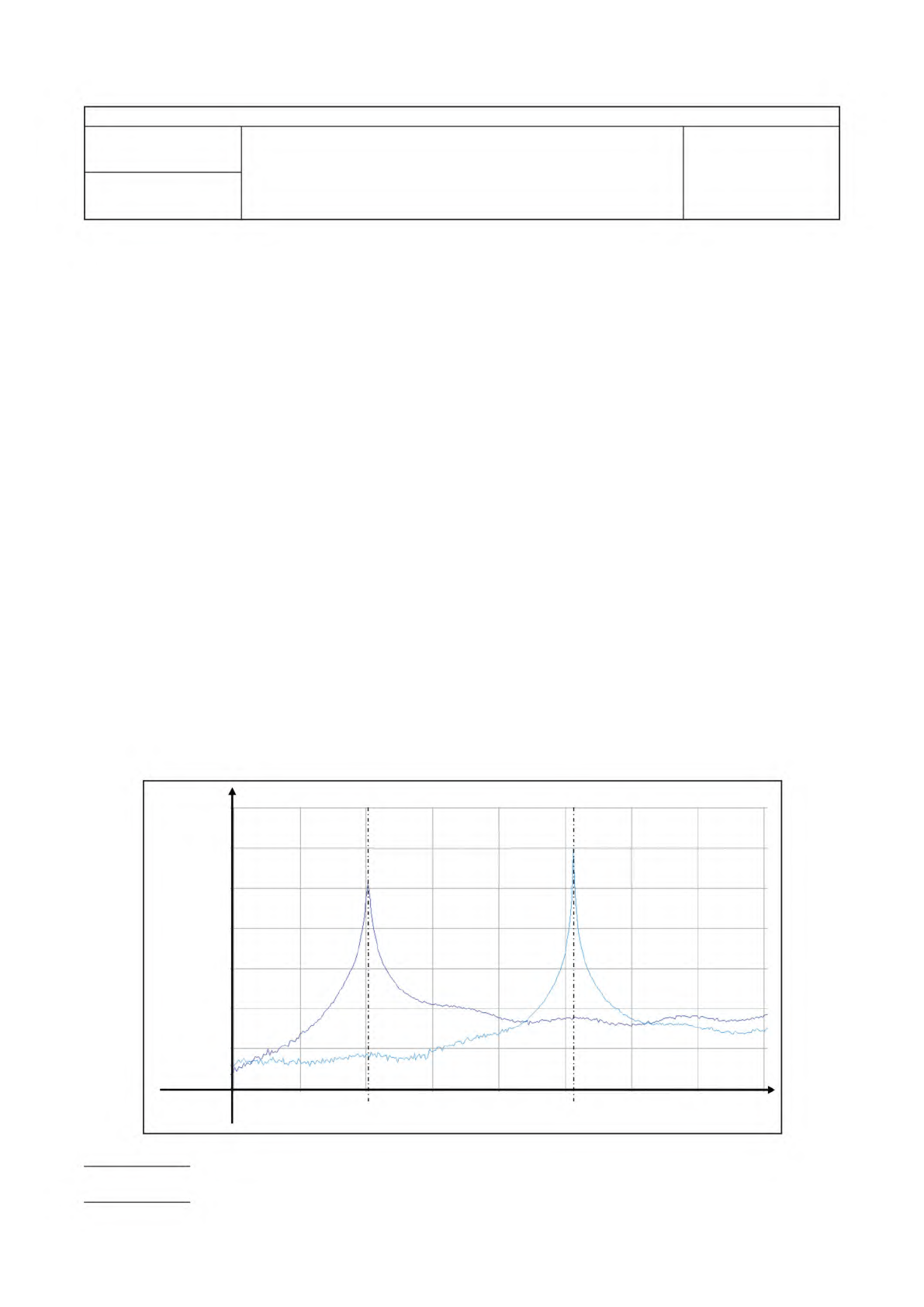
resonance frequency with or without the specimen is shown in Figure 3.
Resonance
amplitude
f
r
f
Resonance
frequency
0
Empty resonator
Resonator
containing the
specimen
Figure3–PlotShowingChangeofResonanceFrequency
2.5.5.15
RelativePermittivityandLossTangentUsinga
06/22
Split-PostDielectricResonator
N/A
Page 4 of 7
―
IPC-TM-650
Number Subject Date
Revision
5.2.7 Calculation
It is recommended to use the computer software provided by the equipment supplier for this calculation. If software not
available, the Relative Permittivity and Loss Tangent at room temperature shall be calculated using the formula shown below.
The relative permittivity (
e
r
) shall be calculated according to Equation (1).
(1)
where
e
r
is relative permittivity;
h is the thickness of the specimen under test, mm;
f
0
is the resonant frequency of empty SPDR Fixture;
f
s
is the resonant frequency of resonator with the dielectric specimen;
K
e
(
e
r
, h) is a function of
e
r
and h. For a fixed resonant cavity, its physical parameters (size, dielectric resonators
e
r
) should have been
identified. K
e
(
e
r
, h) is pre-computed and tabulated by electromagnetic field simulation with the strict Rayleigh-Ritz method. Put
the empty SPDR frequency (f
0
), the resonant frequency with dielectric specimen (f
s
) and the thickness of the specimen (h) under
test into Equation (1). Enter a similar arbitrary value of the relative permittivity of the sample, and use a successive approximation
algorithm. After several iterations, end the calculation when the relative error of the last two calculated relative permittivities is
less than 0.1 %. The last calculated data is taken as the relative permittivity of the specimen.
The loss tangent shall be calculated according to Equation (2).
(2)
where
tan
d
is loss tangent;
Q
s
is the unloaded Q-factor of a resonant fixture containing the specimen;
Q
c
is the Q-factor depending on metal losses for the resonant fixture containing the specimen;
Q
DR
is the Q-factor depending on dielectric losses in dielectric posts for fixture containing the specimen;
p
es
is electromagnetic energy filling factor of the specimen. After identifying the physical parameters of resonant cavity,
the electromagnetic energy filling factor pes can be determined by electromagnetic field simulation. For a fixed
resonant cavity, pes is a constant value. Some additional information is showed in Annex B.
5.2.8
Measure the two remaining specimens by repeating steps 5.2.3 through 5.2.7.
5.2.9
If another test frequency is selected, change the SPDR test fixture in accordance with the test frequency. And then repeat
steps 5.2.2 through 5.2.7.
5.3
Testing of relative permittivity and loss tangent at variable temperatures
5.3.1
The ambient test temperature should be 23 °C ± 2 °C [73.4 ± 3.6 °F]. The variation should not exceed 1°C [1.8 °F] during
the test. Allow at least 30 minutes for the VNA to warm up.
5.3.2
Select a SPDR test fixture in accordance with the test frequency. The specimen size and thickness shall comply with
requirements specified in Table 1. For example, if the test frequency is 10 GHz, a SPDR test fixture with 10 GHz nominal
frequency should be selected. The supported specimen size is 80 mm × 80 mm [3.2 X 3.2 inch] and the maximum thickness
of specimen is no more than 0.9 mm [0.035 inch]. Connect the SPDR test fixture to VNA. The test fixture shall be kept in a
horizontal position in the test chamber. Set the VNA parameters according to the manufacturer’s instructions and the nominal
frequency of the SPDR fixture.
Page 5 of 7
2.5.5.15
RelativePermittivityandLossTangentUsinga
06/22
Split-PostDielectricResonator
N/A
=1
1
/
_/
伉七(
凡㈤
tan
5
(0s
'
-
Qdr
I
-
Cc
I
)
Pes