IPC-TM-650 EN 2022 试验方法--.pdf - 第537页
Both narrow pulse and st ep-source propagation measure- ments are compared with the simulations. D ielectric losses become signif icant mostly on longer lines, while short duration pulses pr opagated on shorter lines hig…
IPC-25512-5-6
0.4
-0.01
0
0.2
0.3
0.1
0 2 4 6 8 10
Measurement
Simulation
0.4
-0.01
0
0.2
0.3
0.1
0 2 4 6 8 10
Measurement
Simulation
Measurement
Simulation
l = 5 cm l = 8 cm
l = 5 cm
l = 20 cm
Time (nsec)
Voltage (V)
Time (nsec)
Voltage (V)
Voltage (V)
0.04
-0.01
0.02
0.03
0.01
0 0.2 0.4 0.6 0.8 1
0
Time (nsec)
Measurement
Simulation
Voltage (V)
0.04
-0.01
0.02
0.03
0.01
0 0.2 0.4 0.6 0.8 1
0
Time (nsec)
Number
2.5.5.12
Subject
Test Methods to Determine the Amount of Signal Loss on
Printed Boards
Date
07/12
Revision
A
IPC-TM-650
Figure
5-6
Typical
TDT
Measurements
and
Validation
Page
16
of
24
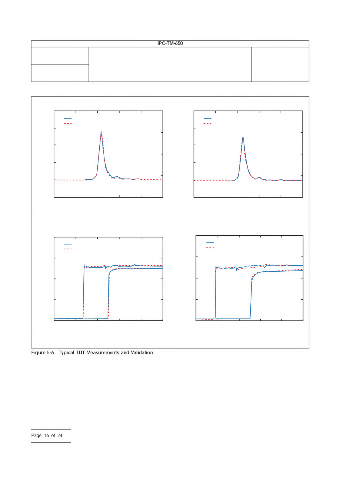
Both narrow pulse and step-source propagation measure-
ments are compared with the simulations. Dielectric losses
become significant mostly on longer lines, while short duration
pulses propagated on shorter lines highlight the good agree-
ment for the high-frequency fit. The agreement in both cases,
both in timing and signal amplitude and shape, perform the
complete validation. In addition, propagation delay measured
on a medium length line, such as 5 cm where losses are not
very strong and end effects are not too significant, can pro-
vide an approximate calculation of ε
r
. This is an approximate
value because the lines are not ideal, losses are present, and
the signal is broadband. However, it gives a bound on the
value of ε
r
that indicates that the disc extraction is not totally
incorrect. The ideal dielectric is then obtained from Equation
5-9.
τ =
√
ε
r
c
[5-9]
where τ is the propagation delay per unit length obtained from
TDT and c is the speed of light in a vacuum. As indicated
before, printed board technology could have fairly large
dimensional tolerances. This is why it is advisable to perform
as many validations of the extracted material parameters as
possible with various approaches, such as the large disc, the
line C, and the TDT-based delay.
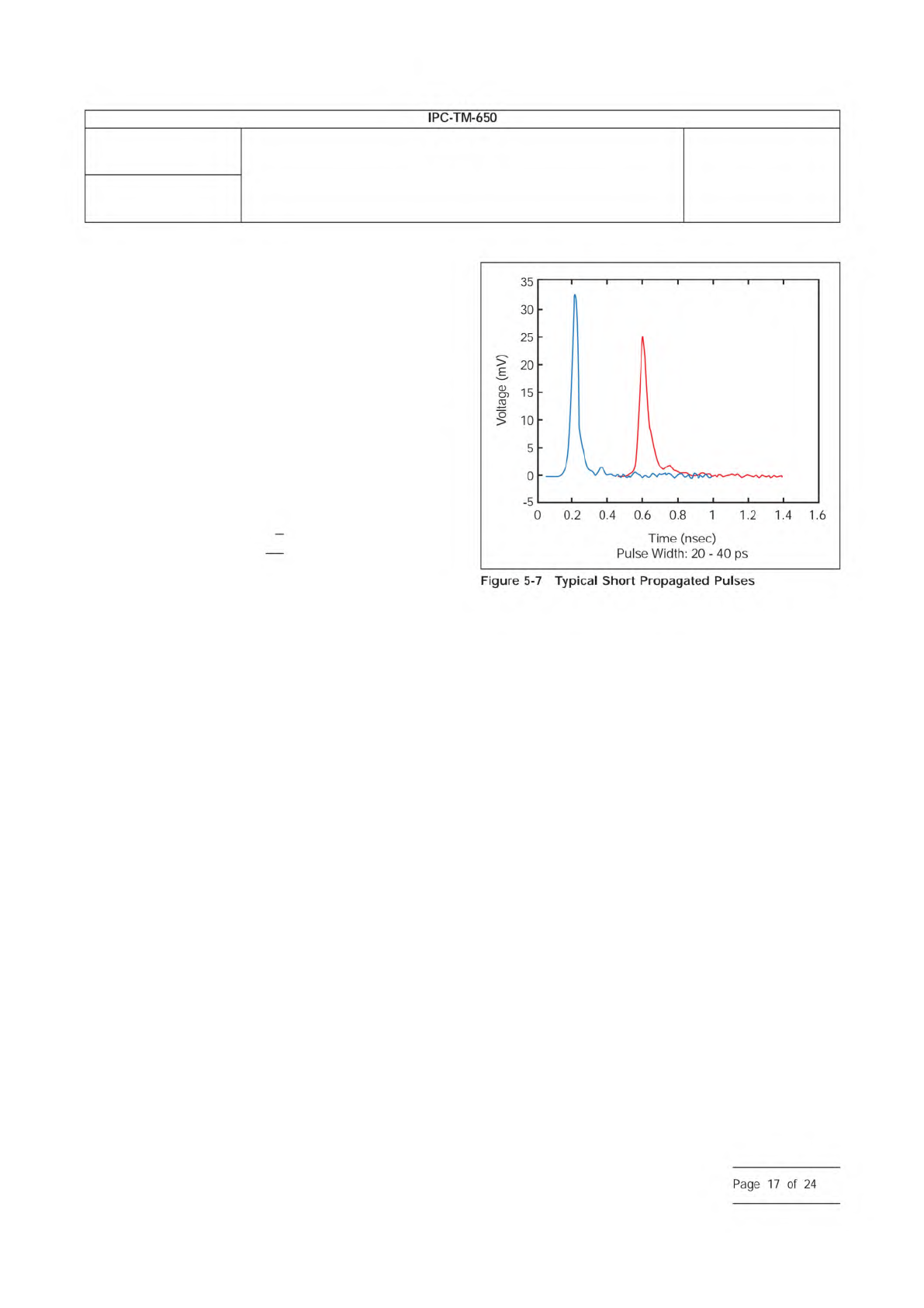
5.3.6 SPP Short-Pulse Measurement
The final type of
electrical measurement is where the technique gets its name.
Pulses of high-frequency content are sent through the con-
ductors, and the output is measured and digitally captured. A
short pulse is created by differentiating a step function. Most
sampling oscilloscopes have suitable step function generation
capability for the general purpose of TDR. Simple passive dif-
ferentiator networks can be placed in-line with the source
cable connecting to the coaxial probes or connectors inject-
ing signal into the printed board. Newer rise time-enhancing
amplifiers can also be placed in-line before the differentiator to
extend the measurement bandwidth. Measurements can be
made with coaxial probes or SMA connector interfaces. A
digitized pulse is measured on each of two lengths of identical
transmission lines. Sample results are shown in Figure 5-7.
Care needs to be taken to use the highest appropriate band-
width cables, probes, adapters; the smallest and shortest
vias, the smallest pads; highest bandwidth detector circuit;
and fastest differentiator (IFN).
Pulses are measured with 512 to 1024 point resolution. The
recommendation is to have 1024 points of timing resolution. It
is acceptable to concatenate captured frames to achieve this.
Typical oscilloscope time base settings are in the range of
25-75 ps/div, depending on the equipment used and length of
lines. The vertical scale is set to maximize use of the screen
while ensuring the entire waveform is captured. It is recom-
mended that captured waveforms consist of 256 averages.
Pulses are generally shifted toward the left of the oscilloscope
screen with just enough of a base DC portion to establish the
correct base reference level. A good rule of thumb is to have
the peak of the pulse reside at the 2nd major horizontal divi-
sion on the screen. The inclusion of the right hand tail of the
signal permits the capture of as much low frequency spectral
content as possible in one frame. The selection of the time per
division setting is then a compromise between having very
high time resolution for the fast portion of the pulse itself and
the need to include the return to ground tail end of the pulse
in less than two frames. The use of more than 1024 horizon-
tal points is not recommended.
The signal line impedance is designed to match the measure-
ment environment of 50 Ω, but this is not absolutely neces-
sary. Different impedances are tolerated, but large differences
may generate too large of an interface reflection that cannot
be eliminated by time-windowing of the Fourier transforms
and could also distort the pulse shapes. The above examples
are considered extremely clean.
The amplitude of the propagated signal should be maximized
through proper contact during probing. If using a probe sta-
tion, this is accomplished through use of proper down force.
IPC-25512-5-7
Number
2.5.5.12
Subject
Test Methods to Determine the Amount of Signal Loss on
Printed Boards
Date
07/12
Revision
A
IPC-TM-650
-5
0
0.2
0.4
0.6
0.8
1
1.2
1.4
1.6
Time
(nsec)
Pulse
Width:
20
-
40
ps
Figure
5-7
Typical
Short
Propagated
Pulses
5
0
5
0
5
0
5
3
3
2
2
1
1
>
E)
o
>
Page
17
of
24
If bolting the SMA connectors on in free space, one needs to
position the DUT to ensure the maximum peak signal.
5.3.6.1 SPP Signal Processing
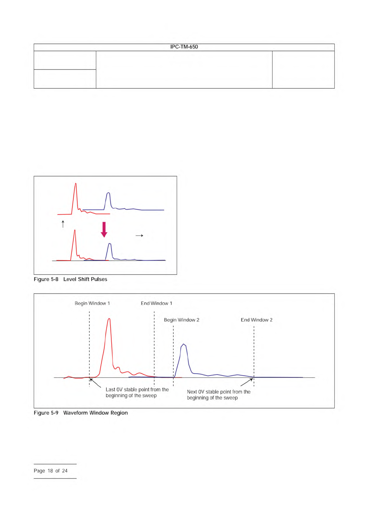
5.3.6.1.1 Level Shifting
The first step is to shift the two
pulses to a common level. Both pulses are shifted to a 0V
level as shown in Figure 5-8. Some pulses will have an initial
offset due to excessive DC drop in the system.
5.3.6.1.2 Time Windowing
Time windowing is required
before the subsequent step that uses a Fast Fourier Trans-
form (FFT). The two waveform windows are defined as a
region of time that starts at the last stable point around 0V for
each conductor and ends next to the stable point around 0V
on the long conductor, as illustrated in Figure 5-9. It is recom-
mended to first determine the extent of Window 2 for the long
line and then use the same extent for the short line, such that
Window 1 and Window 2 are identical.
5.3.6.1.3 Time Shifting and Padding
The next step is to
utilize the window to shift both waveforms by the same delay
so that the beginning of Window 1 is at 0 seconds. Subse-
quently all waveform samples not in the windows are set to 0V
and are called padding. Figure 5-10 provides an example.
5.3.6.2 Fourier Transformation
The Fourier transform is
performed on the two time shifted pulses using the same
number of points as were used in the time-shifting and pad-
ding step (this is important). The number of points must be a
power of 2; a typical number of steps is 8192 or 16384.
Re-sampling is normally required to meet this requirement.
V1(t) is the shifted and padded waveform that represents the
short line of length l
1
and V2(t) is the shifted and padded
waveform that represents the long line of length l
2
. The FFT of
IPC-25512-5-8
Time
Voltage
0V
IPC-25512-5-9
Number
2.5.5.12
Subject
Test Methods to Determine the Amount of Signal Loss on
Printed Boards
Date
07/12
Revision
A
IPC-TM-650
Page
18
of
24