IPC-TM-650 EN 2022 试验方法--.pdf - 第557页
1 Scope This t est method is used to determine the mois- ture and insulation resistances of applied polymer so lder mask under two separate presc ribed conditions of t emperature and humidity. One condi tion i s describe…
frequencies where the conductor losses dominate. Addition-
ally, in the high frequency range, the smoothing may preserve
unrealistic features of the de-embedded insertion loss.
5.4.2 Cumulative Dielectric and Conductor Loss Fit-
ting
As it has been discussed in [14], the cumulative dielec-
tric and conductor losses can be generally approximated by
IL
dB
(,) = a
√
, + b, + c,
2
(Eq. 6)
where , is the frequency in GHz and a, b and c are constants.
For most of the cases coefficient c << 1 and can be
neglected. Therefore, as a first approximation the total loss
curve can be fitted to
IL
dB
(,) = a
√
, + b, (Eq. 7)
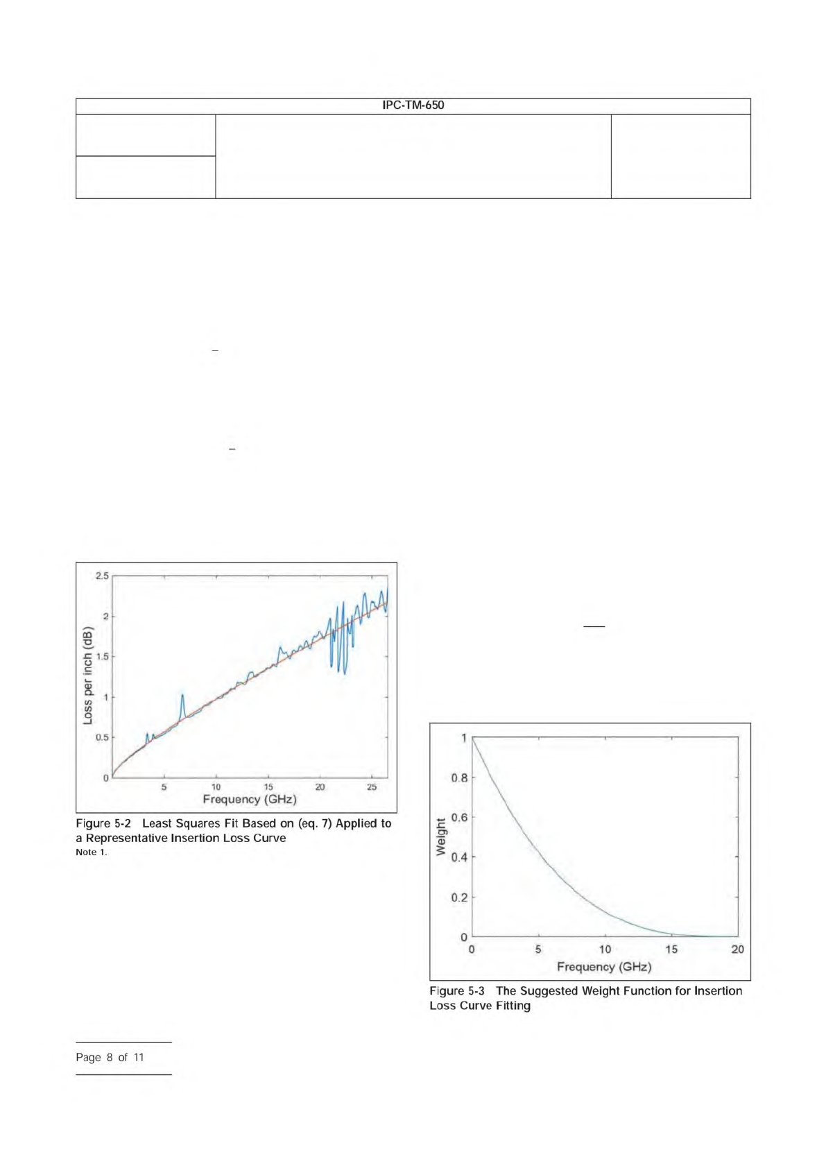
There are number of algorithms that can be used to perform
the printed board loss fit to Eq. 7. One of the most well-known
and widely available algorithms is the least squares fit,
example of which is shown in the Figure 5-2 below.
Even though least squares generally provide a good curve
approximation with the specified behavioral function, there are
many other fitting algorithms that can be applied.
5.4.3 An Alternative Cumulative Dielectric and Conduc-
tor Loss Fitting
Alternatively, when losses cannot be fitted
to the conventional physical based behavioral functions in (Eq.
6) and (Eq. 7), especially when measurement raw data has
high ringing resonances, other empirical approximations can
be used. Fox example, in [15], the following function is set as
the target function for the fitting algorithm:
IL
dB
(,) = a(, – ,
0
)
b
+ c(, – ,
0
)
2
+ d(, – ,
0
) + IL
0
(Eq. 8)
The first term represents the AC conductor loss (i.e., the skin-
effect losses), where ‘b’ is an additional fitting parameter
(instead of a constant 0.5 where ideal conductor loss is a
function of ,
0.5
) added to take into account the surface rough-
ness impact of the conductor. The second and the third terms
represent dielectric losses, and the constant represents the
conductor’s DC loss. Furthermore, a certain offset point (,
0
,
IL
0
) is introduced, where ,
0
is the first frequency point of the
measurement. The offset is added to accommodate the fact
that VNA measurements made at the printed board fabricator
usually do not provide results lower than 10 MHz.
The abovementioned methods fit the data to a smooth curve
over the entire bandwidth of the measurement where each
data point is allocated equal weight. As measurement errors
usually increase significantly at high frequencies, a weighting
scheme can be introduced to force the algorithm to prioritize
the curve fitting at the low frequencies and minimize (or ignore)
the impact of high frequency:
W(,) =
(
1–
(
,
,
max
))
3
(Eq.9)
where ,
max
is the maximum measurement frequency. Figure
5-3 shows the suggested weighted function where ,
max
= 20
GHz.
IPC-25514-5-2
Red represents the fitted curve.
IPC-25514-5-3
Number
2.5.5.14
Subject
Measuring High Frequency Signal Loss and Propagation on
Printed Boards with Frequency Domain Methods
Date
02/2021
Revision
IPC-TM-650
Figure
5-2
Least
Squares
Fit
Based
on
(eq.
7)
Applied
to
a
Representative
Insertion
Loss
Curve
Note
1.
Figure
5-3
The
Suggested
Weight
Function
for
Insertion
Loss
Curve
Fitting
.5
2
.5
1
.5
O
2
L
S
s
p)
uow
j
d
SSO1
Page
8
of
11
1 Scope
This test method is used to determine the mois-
ture and insulation resistances of applied polymer solder mask
under two separate prescribed conditions of temperature and
humidity. One condition is described as Class T and the other
Class H. Raw material qualification testing is performed on
designated comb patterns. Production quality conformance
testing is performed on a standard ‘‘Y’’ pattern.
2 Applicable Documents
Multipurpose One-Sided Test Pattern -
Gerber Format
Qualification and Performance of Permanent
Solder Mask
Requirements for Soldering Fluxes
Acceptability for Printed Boards
3 Test Specimens
The IPC-A-25A-G-KIT artwork package
provides the Gerber files necessary for the fabrication of the
standard IPC-B-25A test board used with this test method.
3.1 Qualification Testing
3.1.1 Class H
Three IPC-B-25A boards using the D comb
patterns with 0.32 mm [0.0126 in] lines/spaces (see Figure 1).
Of which, two are to be coated and one uncoated with solder
mask according to the solder mask supplier’s recommenda-
tions.
3.1.2 Class T
Three IPC-B-25A boards using the E and F
comb patterns with 0.41 mm [0.016 in] lines and 0.51 mm
[0.020 in] spaces (see Figure 1). Of which, two are to be
coated and one uncoated with solder mask according to the
solder mask supplier’s recommendations.
3.2 Conformance Testing
IPC-B-25A board C (‘‘Y’’
shape) pattern with 0.64 mm lines/0.64 mm spacing [0.025 in
lines/0.025 in spacing] or pattern with minimum spacing on
the production board (see Figure 1), whichever has the small-
est line spacing, coated with solder mask according to the
solder mask suppliers recommendations.
4 Apparatus
4.1 Chamber
A clean chamber capable of programming
and recording an environment of 25 ± 2 °C [77 ± 3.6 °F] to at
least 65 ± 2 °C [149 ± 3.6 °F] and 90-98% relative humidity.
This test requires a clean chamber and clean water
for repeatable test results. The following recommendations
are made:
• Incoming water purity should be between 0.5 and 0.1
micro-siemens/cm.
• Fresh deionized water should be used for each test, rather
than using a recirculating water sump.
• Chamber workspaces should be cleaned at least every six
months.
1. www.ipc.org/onlinestore
IPC-2631-1
3000 Lakeside Drive, Suite 309S
Bannockburn, IL 60015-1249
IPC-TM-650
TEST METHODS MANUAL
Number
2.6.3.1
Subject
Solder Mask - Moisture and Insulation Resistance
Date
03/07
Revision
E
Originating Task Group
Solder Mask Performance Task Group (5-33b)
ASSOCIATION CONNECTING
ELECTRONICS INDUSTRIES
®
IPC-A-25A-G-KIT1
IPC-SM-840
J-STD-004
IPC-A-600
Figure
1
IPC-B-25A
Test
Board
NOTE:
Material
in
this
Test
Methods
Manual
was
voluntarily
established
by
Technical
Committees
of
IPC.
material
advisory
only
and
its
use
or
adaptation
,
s
entirely
voluntary.
IPC
disclaims
all
liability
of
any
kind
as
to
the
use,
application,
or
adaptation
of
this
material.
Users
are
also
wholly
responsible
for
protecting
themselves
against
all
claims
or
liabilities
for
paten!
infringement.
Equipment
referenced
/s
the
convenience
of
the
user
and
does
not
imply
endorsement
by
IPC.
Page
1
of
5
Note that an uncertainty estimate of 15% (as an example) is
not meant to suggest that the true insertion loss is within 15%
of the reported value. Rather, the uncertainty estimate is
merely an indicator for the amount of measurement and
de-embedding error evident at any given point.
5.4.5 Determine the Usable Bandwidth of Reported
Insertion Loss
The uncertainty level described in 5.4.4 can
be used to determine the usable bandwidth of the reported
insertion loss. The user can set up an acceptable uncertainty
level based on a specific application, and then examine the
reported insertion loss value at various frequencies, to deter-
mine its usable bandwidth of reported insertion loss (where
the uncertainty level is smaller than the pre-set value).
5.5 Verification of Reported Insertion Loss
Due to
manufacturing variation, and the uncertainties associated with
the calibration/de-embedding process, it is desirable to make
multiple measurements of the same coupon design to
improve the confidence of the measurement results. This is
critical when the material is in a qualification stage and the
amount of manufactured coupons is limited.
One simple approach to verify the reported insertion loss is to
design coupons with multiple lengths on the same board: L1,
L2, and L3. The de-embedding process outlined in 1.2.2 and
1.3 can be applied to any two length combinations:
IL
unit_12
=
|e
-γ (L2–L1)
|
L2–L1
(Eq. 12)
IL
unit_23
=
|e
-γ (L3–L2)
|
L3–L2
(Eq. 13)
IL
unit_13
=
|e
-γ (L3–L1)
|
L3–L1
(Eq. 14)
It is desirable to have the reported insertion loss per unit
length being consistent (e.g., within 5% of each other). A large
discrepancy indicates either problems in measurement/de-
embedding procedures, or a large manufacturing variation
across the board. An average of the above insertion loss num-
ber can be used to report the final value.
It is also important to note that keeping a large length differ-
ence between any two lengths among L1, L2, and L3 will also
help to improve the quality of reported insertion loss.
5.6 Temperature Impact of Insertion Loss
It is known
that the copper conductivity decreases, and the loss tangent
of dielectric material increases with the increase of environ-
mental temperature. Therefore, the insertion loss increases
with the increase of temperature. Meanwhile, the temperature
impact on insertion loss varies with different printed board
materials.
A Test chamber with variable temperature setting is needed.
A suggested temperature range is 0 °C ~ +100 °C, or other-
wise specified by the tester. Temperature accuracy is < ± 1 °C
of actual set point. Humidity accuracy is < ± 5% RH of actual
set point, or otherwise specified by the tester.
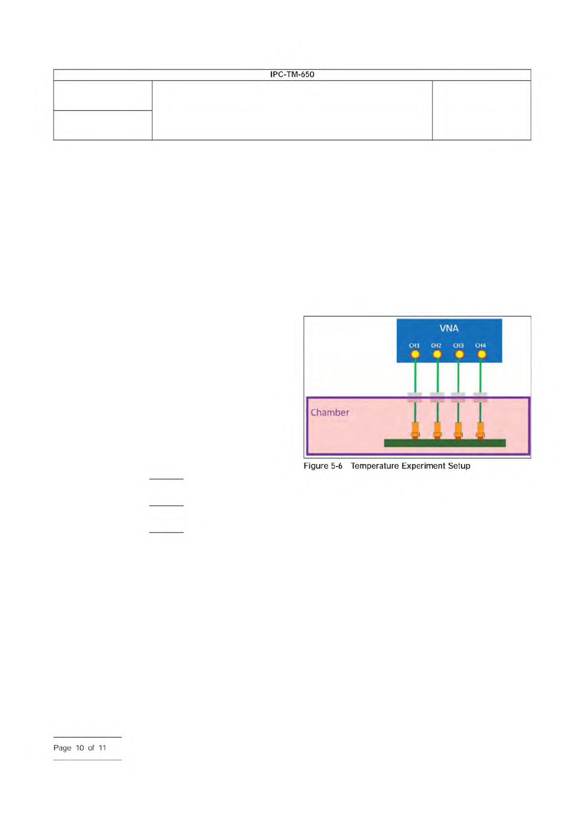
It is recommended to use phase-stabilized cables for tem-
perature ranges of 0 °C ~ +100 °C, or otherwise specified by
the tester. Figure 5-6 provides an example of a temperature
experiment setup.
The following procedures describe how to quantify the tem-
perature impact for a given printed board material:
1) Set up VNA equipment according to 5.1.
2) Bake the test coupon at 120 °C over 6 hours.
3) Calibration VNA equipment to the end of cable with
co-axial connector SOLT standards, with the cable
stayed outside the environment chamber.
4) Move cable end through the conduit of chamber and
connect to the long trace of DUT inside the chamber.
Make sure the conduit is sealed with thermal resistant
material after the cable penetrates the chamber. (Note:
high temperature resistant cable should be used)
5) Set the chamber to the target testing temperature and
humidity.
6) Wait at least half an hour to ensure DUT is set to the
ambient temperature
7) Conduct measurement and record data.
8) Moving to the next temperature and humidity setting
(Step 5), until results of all settings are recorded.
IPC-25514-5-6
Number
2.5.5.14
Subject
Measuring High Frequency Signal Loss and Propagation on
Printed Boards with Frequency Domain Methods
Date
02/2021
Revision
IPC-TM-650
Figure
5-6
Temperature
Experiment
Setup
Page
10
of
11