IPC-TM-650 EN 2022 试验方法--.pdf - 第552页
structure are measured first. Assuming the 2X -Thru structure is symmetric, the S-parameters of a 1X structure can be cal- cul ated directly from the 2X-Thru measurement . Once the S-parameters of the 1X structure on bo …
available based on equation (1). Note that the de-embedded
insertion loss is defined with a reference impedance of the
transmission line.
1.3 General Calibration/de-embedding Methods to Set
up Correct Reference Plane for Printed Board Conduc-
tor Insertion Loss Characterization
As mentioned earlier,
there are existing calibration/de-embedding methods for gen-
eral purpose interconnect characterization to move the cali-
bration reference plane to printed board interfaces. These
methods are validated by the industry, and therefore included
herein, although they are either more complicated or costly
than the Eigen-value based method.
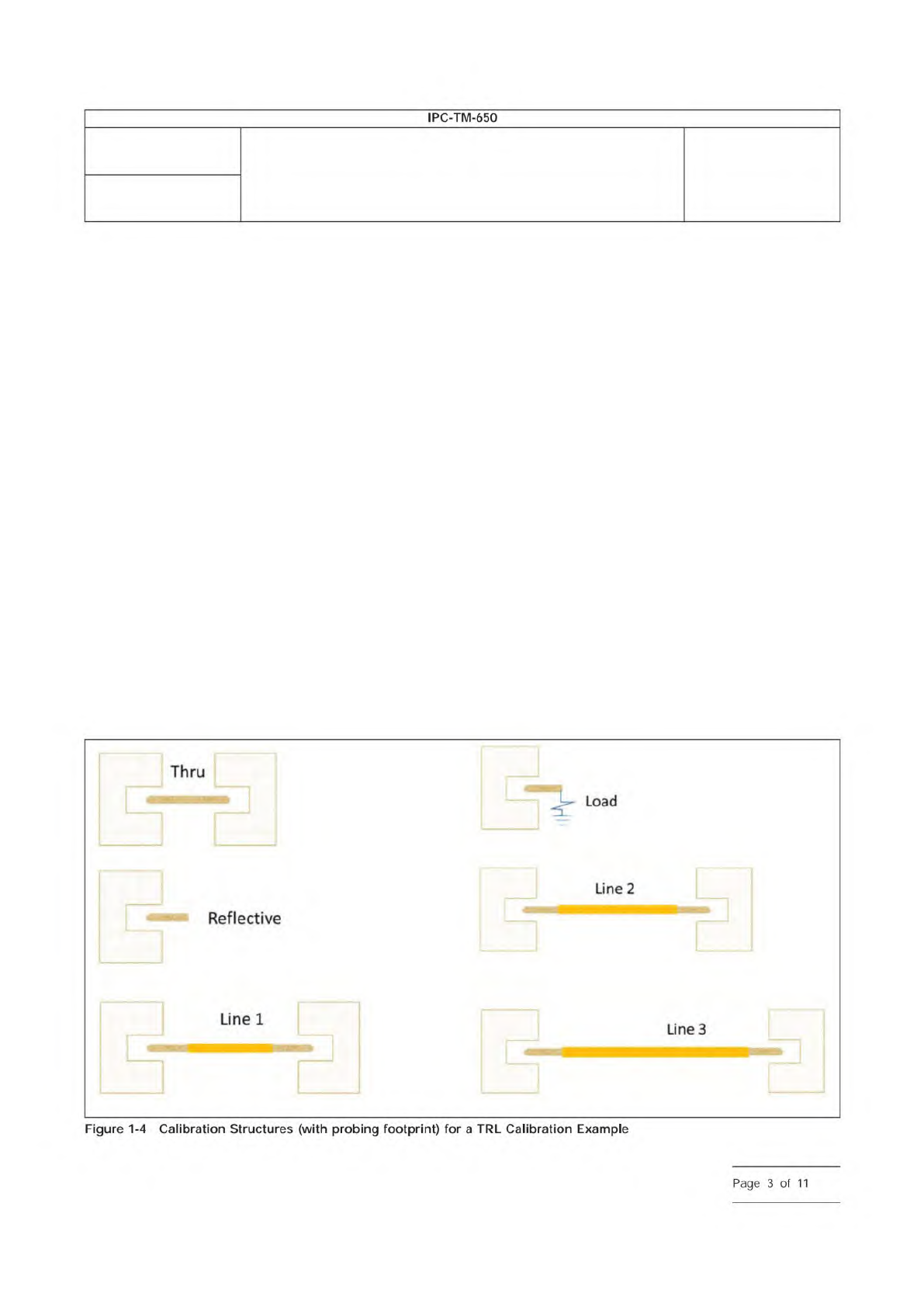
1.3.1 TRL Calibration
The TRL (and its variants such as
LRM) method [7] is a general approach to move the calibra-
tion reference plane from the coaxial connector to printed
board interfaces. Figure 1-4 shows the typical calibration
structures for a TRL calibration, with microwave probe foot-
print (with single-ended probing as an example). The TRL cali-
bration technique only relies on the characteristic impedance
of the transmission line and does NOT need the parasitics of
Reflective Standard to be known, nor propagation delay of
Line. A typical TRL calibration structure may also include a
Load structure that works only at very low frequencies, and
additional Line structures to cover a wide frequency range.
Most VNAs offer TRL calibration options, please refer to the
manual or application note for your specific equipment to per-
form a TRL calibration.
TRL calibration has been widely used in the industry since the
technique no longer requires accurate calibration termination
standards. This overcomes the difficulties of SOLT calibration,
and the reference plane can be moved to the printed board.
However, there are still some disadvantages to the TRL cali-
bration. For example, there are many components of the cali-
bration standard to handle. This takes substantial printed
board area and requires tedious calibration process in the lab,
while being prone to the operator error. Additionally, the TRL
technique requires accurate characteristic impedance specifi-
cation for the line standard, which is problematic to determine
in a dispersive environment.
1.3.2 2X-Thru De-embedding
In the last decade, the
2X-thru de-embedding methodology is gaining popularity due
to its simplicity of test fixture design and de-embedding pro-
cedures [8]. In contrast to the TRL calibration technique,
which requires measurement of multiple structures as shown
in Figure 1-4, 2X-Thru De-embedding requires only one
de-embedding structure.
The basic idea of the 2X-Thru de-embedding approach is
shown in Figure 1-5. The S-parameters of the 2X-thru
IPC-25514-1-4
Number
2.5.5.14
Subject
Measuring High Frequency Signal Loss and Propagation on
Printed Boards with Frequency Domain Methods
Date
02/2021
Revision
IPC-TM-650
—
Thru
Reflective
Line
1
Figure
1-4
Calibration
Structures
(with
probing
footprint)
for
a
TRL
Calibration
Example
Page
3
of
11
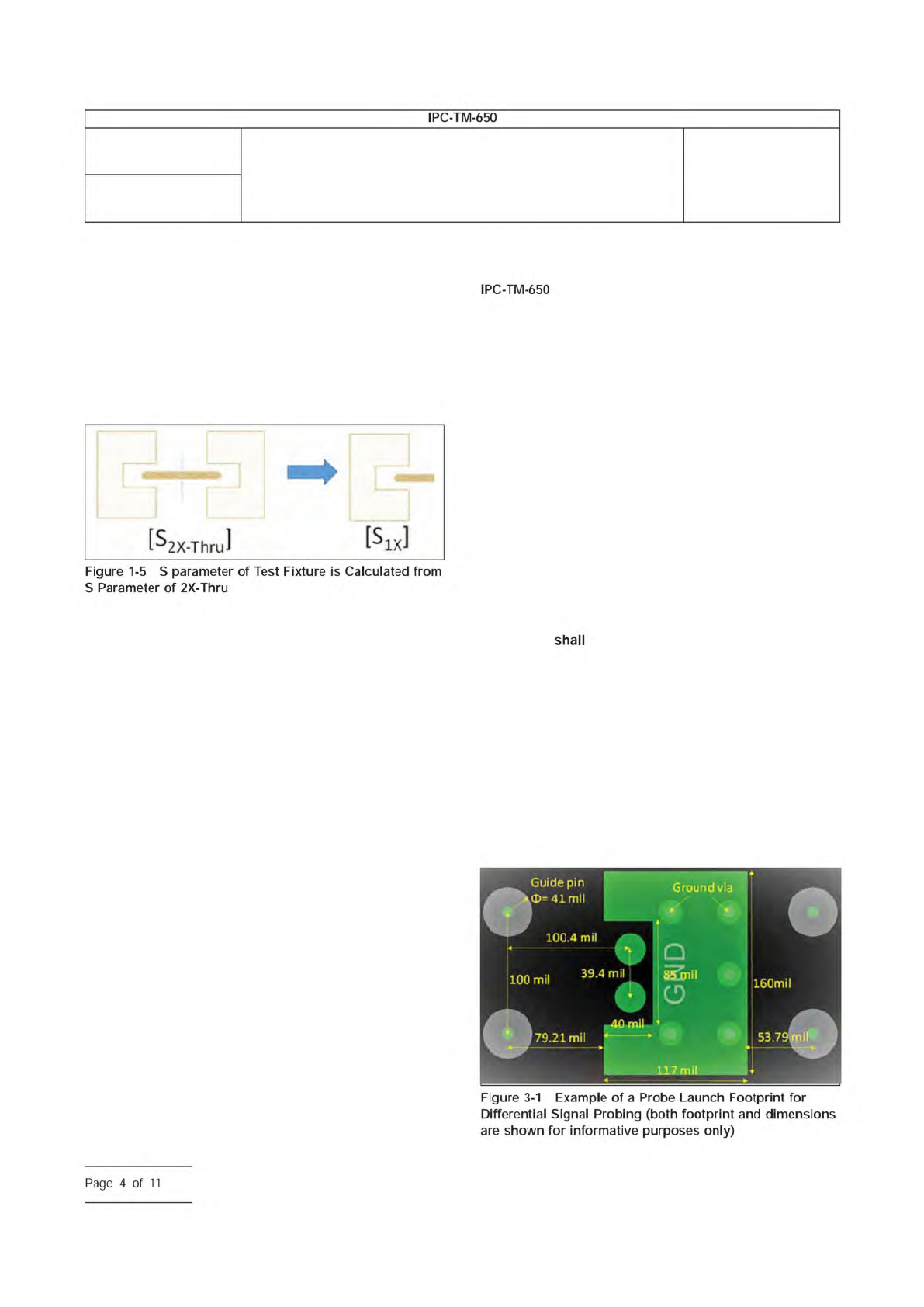
structure are measured first. Assuming the 2X-Thru structure
is symmetric, the S-parameters of a 1X structure can be cal-
culated directly from the 2X-Thru measurement. Once the
S-parameters of the 1X structure on both sides on the DUT
are obtained, the S-parameters of the DUT can be readily cal-
culated. This significantly simplifies calibration/de-embedding
procedures as compared to a traditional TRL calibration
where six calibration structures are typically needed.
There are various 2X-Thru de-embedding tools available at
time of publication of this test method, such as [9][10][11]. The
accuracy of 2X-Thru de-embedding tool is has been shown to
be comparable to TRL [13]. However, since the algorithm of
commercially available 2X-Thru methods are often proprietary,
it is up to the users to validate the tool for their printed board
insertion loss measurements. IEEE 370-2020 addressing this
issue by setting up a process to validate the de-embedding
tools [12]. Below is the general process of using 2X-Thru
de-embedding process to measure the insertion loss:
1) Manufacture two printed board conductors with different
lengths (L1 and L2).
2) Perform SOLT calibration to move reference plane to the
end of coaxial connector.
3) Perform VNA measurement and to acquire the S param-
eters of the shorter conductor (L1) and longer trace (L2).
4) Use 2X-Thru tool to de-embed the S parameters of L2,
while treating the shorter conductor L1 as test fixture. This
end up with S parameters of a transmission line DUT of
length L2-L1.
5) Renormalize the S parameter using the characteristic
impedance of transmission line.
6) The renormalized S21 represents the insertion loss of DUT
(length of L2-L1).
2 Applicable Documents
Test Methods Manual
2.5.5.12 Test Methods to Determine the Amount of Signal
Loss on Printed Boards
3 Test Specimens
3.1 Common Test Coupon Characteristics
The test
coupon contains two or more transmission lines. The follow-
ing are general guidelines for designing transmission line test
structures for the test methods within this document. These
transmission line test structures may be placed within the
functional area of the printed board or within test coupons. It
is recommended that coupons have labels that contain infor-
mation about the associated test line signal layer; for example,
L1, L3, etc. Labeling of the contact land for differential
conductors shall clearly indicate the matched pair. It is recom-
mended that test coupons include a printed board serial num-
ber, part number, and date code.
3.2 Ground and Reference Planes
All reference planes in
the coupon
be connected together within the coupon
area and be independent of those planes in the functional cir-
cuit area.
3.3 Probe Launch Footprint
The probe launch footprint is
comprised of signal pads and ground contact. Each probe
vendor can specify its optimized probe launch footprint. How-
ever, it is desirable to have footprint that is compatible with
multiple probes. Figure 3-1 shows an example of a differential
probe launch footprint compatible with both micro- and hand-
held probes. A similar single-ended probe launch footprint is
shown in Figure 3-2, with the same guide pin design.
IPC-25514-1-5
IPC-25514-3-1
Number
2.5.5.14
Subject
Measuring High Frequency Signal Loss and Propagation on
Printed Boards with Frequency Domain Methods
Date
02/2021
Revision
IPC-TM-650
—
IPC-TM-650
Figure
1-5
S
parameter
of
Test
Fixture
is
Calculated
from
S
Parameter
of
2X-Thru
Figure
3-1
Example
of
a
Probe
Launch
Footprint
for
Differential
Signal
Probing
(both
footprint
and
dimensions
are
shown
for
informative
purposes
only)
Page
4
of
11
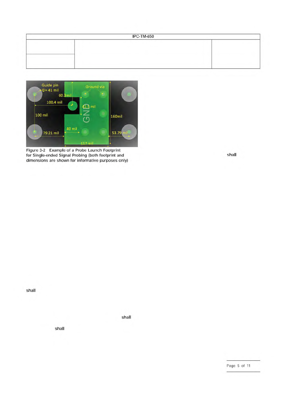
It is important to note that these are just footprint examples,
and the electrical performance of these footprint may be fur-
ther improved based on the layer stackup, such as voiding the
ground plane right beneath the signal pads. Each probe ven-
dor can specify its optimized probe launch footprint that
meets the electrical requirement specified in 4.2. Furthermore,
it is critical to work with probe vendor to make sure the fin-
ished drill hole size is compatible with the probe.
Note that the footprint example shown in Figure 3-1 is appli-
cable for measurements up to 20GHz and that the footprint
can be further optimized for application at higher frequencies.
3.4 Connector Launch
Alternative to microwave probes,
high bandwidth connector launch may be used instead of
probe launch as show in Figure 3-2 and Figure 3-3 of IPC-
TM-650 Method 2.2.2.12A. Although the hand-held probe
approach is quicker and more convenient to use, the connec-
tor solution is usually more reliable and less prone to human
errors.
3.5 General Surface Condition
The panel test coupons
have the same surface plating and use the same solder
mask requirements as the functional printed board. The plat-
ing of the launch footprint should be suitable for probing or
co-axial connector connection.
3.6 General Routing Guidelines
The test lines be
referenced to a continuous ground/voltage planes. The test
line conductors
be kept at minimum distance Dmin from
printed board structures such as voids, plane splits, other
conductors and holes, where Dmin is six times the height of
dielectric layer (from line conductor to the closest reference
plane) or 2.54 mm [0.100 in], whichever is greater.
Fiber-weave impact should be mitigated unless the intent is to
measure its impact. One mitigation example is to have the test
line routed at about 10 degree angle (or close to the routing
scenario in actual product design) with respect to the fiber-
weave alignment. Alternative, straight routing (parallel to board
edge) can be used if the Gerber image is rotated by about 10
degrees on the panel.
It is recommended to route the test lines with the same cross-
section and target impedance as in the actual product layout.
Thieving, which is the use of non-terminated copper struc-
tures such as planes, pads, and/or conductors adjacent to
test lines that ensure plating consistency, may be used on the
test coupon. All thieving structures (if used)
be placed at
least Dmin away from each test interconnect. It is recom-
mended to make sure copper density at each routing layer is
representative of the actual product.
3.7 Impact of Vias in the Printed Board Conductor Loss
Characterization
Measuring the signal loss for inner layer
(stripline) can be challenging when there is a substantial loss
due to the via or via stub effect. Reducing via effect can
improve the de-embedding results. This can be achieved by:
• Minimizing via stub length by probing from the appropriate
side of the board (from the top for traces on the bottom half
of the board and vice-versa, to assure minimum via stub
length)
• Minimizing via stub length by back-drilling. However, this
needs to be done with good control of back-drilling depth.
Inconsistent back-drilling depth between the vias for two
different routing length can lead to large de-embedding error
• Extra attention needs to be paid to stacked via designs, as
this approach, while avoiding stubs and improving signal
integrity, has high manufacturing variants
• The resonance frequency should be outside of intended
measurement bandwidth
For signals on outer layer (microstrip), the conductor should
be routed without via or via stub.
3.8 Impact of Environmental Condition in the Printed
Board Conductor Loss Characterization
Temperature
and humidity affect loss measurements. It is therefore critical
to clearly document the testing condition in the reported inser-
tion loss.
For insertion loss of conductors routed on outer layer, the
results can be different under the conditions described in
3.8.1 vs. those described in 3.8.2 due to the humidity impact.
IPC-25514-3-2
Number
2.5.5.14
Subject
Measuring High Frequency Signal Loss and Propagation on
Printed Boards with Frequency Domain Methods
Date
02/2021
Revision
IPC-TM-650
—
Figure
3-2
Example
of
a
Probe
Launch
Footprint
for
Single-ended
Signal
Probing
(both
footprint
and
shall
dimensions
are
shown
for
informative
purposes
only)
shall
shall
shall
Page
5
of
11