IPC-TM-650 EN 2022 试验方法--.pdf - 第753页
e) A su rface finish for fine pitch featured PCBs that are often assembled using surface mount components (SMCs) . The OSP surface finish p rovides very flat/co-planar l and a reas for the placement and attachment of SMC…
5.3 Data Handling and Analysis
5.3.1
Lognormal plots are recommended for plotting per-
cent of samples above an insulation resistance value, versus
insulation resistance. Use the log value of the insulation resis-
tance.
5.3.2
If lognormal plots are not used, a test circuit failure
be determined by more than a decade drop in insulation
resistance as a result of the applied bias. The baseline for the
decade drop
be the average insulation resistance at 96
hours for each coupon (A-1, A-2, etc.).
5.3.3
Test board nets with less than 10 megohms insulation
resistance (high resistance short) after the 96-hour stabiliza-
tion
be excluded, since these failures are due to poor
PTH hole quality or laminate capability.
5.3.4
The insulation resistance baseline (before bias condi-
tioning) value for a given daisy-chain net (same design spac-
ing)
be the average resistance of those un-shorted
daisy-chain nets on all test boards in the valid sample group
as measured after the 96-hours stabilization period.
5.3.5
The percent failure rate for a given sample group and
subsequent test condition is the percent of test boards that
show more than a decade drop in resistance compared with
the baseline value for daisy-chain nets with the same design
spacing.
5.3.6
For a given sample lot, there may be binomial failure
distributions where assignable causes exist along with differ-
ent levels of capability.
5.4 Visual Examination
After completion of the test, the
test boards
be removed from the environmental cham-
ber and examined at 10X magnification for evidence of sur-
face insulation resistance failure (i.e., discoloration, corrosion),
handling or processing defects other than CAF.
5.4.1 Assignable Cause
Where an assignable cause of
low insulation resistance can be properly attributed to a han-
dling or processing defect other than CAF (i.e., contamination
on the insulating surface of the board, scratches, cracks, or
other obvious damage affecting the insulation resistance
between the conductors), then such a value should be
excluded.
5.4.2 CAF Microsections
Since CAF filaments form along
the interface between resin and the woven reinforcement,
these filaments can be very small and easily disrupted by a
relatively low current flow or other causes. Microsectioning to
observe CAF filaments can be a tedious process with a low
success rate.
5.5 Reporting Results
5.5.1
The percent failure rate at 500 hours for each spacing
in sections A and B are the results of interest. Generally PWB
processing has the greatest impact on reduced CAF resis-
tance at smaller plated-through hole-to-plated-through hole
(PTH-PTH) spacings, while the laminate material has the
greatest impact at larger PTH-PTH spacings. However, the
laminate material used can also affect the extent of fracturing
and copper wicking near a PTH.
5.5.2
There are several additional factors that can affect
CAF resistance. See APPENDIX A for the list of PCB manu-
facturing parameters that may affect CAF resistance and that
should be documented.
6 Notes
6.1 Definitions [Only those terms not already included in IPC-
T-50.]
a)
The growth of metallic conductive salt filaments by means
of an electrochemical migration process involving the
transport of conductive chemistries across a nonmetallic
substrate under the influence of an applied electric field,
thus producing Conductive Anodic Filaments.
b)
The growth of conductive metal filaments across or
through a dielectric material in the presence of moisture
and under the influence of voltage bias.
c)
This is a multi-functional surface finish wherein the electro-
less nickel layer is capped with a thin layer of immersion
gold. It is applicable to soldering, aluminum wire bonding,
press fit connections and as a contact surface. The
immersion gold protects the underlying nickel from
oxidation/passivation over its intended life.
d)
An underwriters Laboratories Inc. (UL) requirement value
of laminate materials as determined by the results of tests
performed by UL.
Number
2.6.25
Subject
Conductive Anodic Filament (CAF) Resistance Test: X-Y Axis
Date
02/21
Revision
C
IPC-TM-650
shall
shall
shall
shall
Conductive
Anodic
Filament
(CAF)
Formation:
Electrochemical
Migration
(ECM):
shall
Electroless
Nickel
/
Immersion
Gold
(ENIG):
Maximum
Operating
Temperature
(MOT):
Page
8
of
11
e)
A surface finish for fine pitch featured PCBs that are often
assembled using surface mount components (SMCs). The
OSP surface finish provides very flat/co-planar land areas
for the placement and attachment of SMC devices.
f)
This phrase alludes to the manufacturing of a bare printed
circuit board that is not populated (assembled) with any
discrete components.
6.2 Reference Documents
Electrochemical Migration: Electrically Induced
Failures in Printed Wiring Assemblies
Electrochemical Migration
Resistance Test (note: covers only surface electrochemical
migration)
Surface Insulation Resistance Handbook
Number
2.6.25
Subject
Conductive Anodic Filament (CAF) Resistance Test: X-Y Axis
Date
02/21
Revision
C
IPC-TM-650
—
Organic
Solderability
Preservative
(OSP):
Printed
Circuit
Board
Fabrication
(PCB
Fab):
IPC-TR-476
IPC-TM-650,
Method
2.6.14.1
IPC-9201
Page
9
of
11
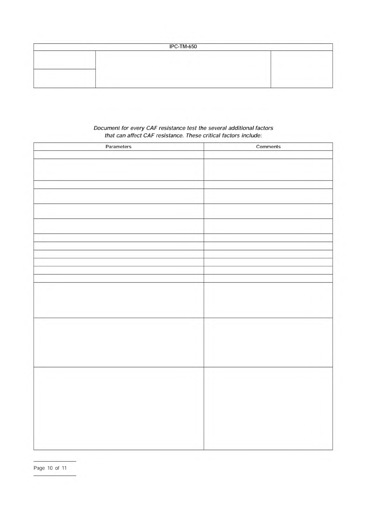
APPENDIX A
Additional CAF Resistance Factors Checklist
Test board part number and revision level.
Drilled Hole Size for each Hole-Hole and Hole-Plane spacing tested (also
recommend drilling feed rate, speed of rotation, chip loading data, backup
material type, etc.).
Desmear & Cleaning Process (ex: permanganate, plasma).
Whether glass microetch was used (and if so, the controlling process
parameters).
Board finish type (HASL or specific OSP, immersion silver, immersion tin,
ENIG, etc.).
Laminate material type that was used (manufacturer and material name or
number).
Woven Glass Manufacturer (silane treatment application).
Type of soldermask (if used).
PCB Fab manufacturer and facility.
Method of separating test board from working panel.
Number of circuit layers in test board.
Copper thickness in plated through holes in test board.
Dielectric Thickness and Construction (same construction throughout is
recommended for CAF testing). Examples:
Core 2/2 3.0 mils thick 1 ply 1080, Prepreg 1 ply 1080
Core 1/1 4.3 mils thick 1-106/1-1080, Prepreg 1-106/1-1080
Core H/H 5.0 mils thick 1-2113, Prepreg 1-2113
Failure Location (with examples)
Glass-Resin Boundary
Migration Between Glass Fibers
Migration Between Fiber Bundles
Void within Fiber Bundle
Incomplete Wetting Against Fiber
Hollow Fiber (report glass cloth supplier name, name of fiber source)
Test Interruptions:
Cause (example: power interruption)
Length of Interruption
Test Re-Start Parameters
Frequency of Measurement. Examples:
24 Hours
20 Minutes
6 Minutes
Time of Failure: Examples
200 Hours (hollow fiber)
300 Hours (void within fiber bundle)
21 Hours (migration between fiber bundles)
Number
2.6.25
Subject
Conductive Anodic Filament (CAF) Resistance Test: X-Y Axis
Date
02/21
Revision
C
IPC-TM-650
Document
for
every
CAF
resistance
test
the
several
additional
factors
that
can
affect
C4F
resistance.
These
critical
factors
include:
Parameters
Comments
Page
10
of
11