IPC-TM-650 EN 2022 试验方法--.pdf - 第746页
IPC-9253 and IPC-9254 Test Structures A 1 through A4 The four str uctures A1-A4 each have five rows of connected vias. Within ea ch st ructure each row has 42 vias with alternat- ing rows bein g tied to po sitive or nega…
1 Scope
This test method provides a means to assess the propensity
for conductive anodic filament (CAF) growth and other forms
of electrochemical migration failure modes within a printed
board (PB). This test method can be used to assess PB lami-
nate materials, PB design and application parameters, PB
manufacturing process changes and other applications such
as press-fit connectors.
This IPC test method has not been designed for
use with voltages exceeding 100 Vdc bias, however higher
voltage bias testing is being routinely required to be per-
formed, such as for electric vehicle electronics. Note that at
100 Vdc using 20 mA cut-off means 2 watts of power being
dissipated per channel, so using a much lower cut-off current
is recommended for better root cause failure analysis.
As voltage bias is increased, the wiring insulation
required needs to change in order to ensure operator safety.
2 Applicable Documents
2.1 IPC
CAF Test Board Design (Available in the ‘‘Drafts’’
section of the 5-32e Task Group Home Page)
CAF Test Board Design (Available in the ‘‘Drafts’’
section of the 5-32e Task Group Home Page)
CAF Test Board Design (Available in Free Down-
loads in IPC Home Page)
CAF Test Board Design (Available in Free Down-
loads in IPC Home Page)
CAF Test Method User Guide for the IPC-TM-650,
Method 2.6.25
Requirements for Soldered Electrical and
Electronic Assemblies
Requirements for Soldering Fluxes
Requirements for Electronic Grade Solder
Alloys and Fluxed and Non-Fluxed Solid Solders for Electronic
Soldering Applications
2.3.25 Detection and Measurement of Ionizable Surface
Contaminants by Resistivity of Solvent Extract
2.6.27 Thermal Stress, Convection Reflow Assembly
Simulation
2.2 American Society for Testing and Materials (ASTM)
Standard Test Methods for DC Resistance or
Conductance of Insulating Materials
3 Test Specimens
The IPC-9254 CAF test board design is the older coupon and
has been superseded by the IPC-9253. The new smaller CAF
test coupons are IPC-9255 and IPC-9256 and are used for
evaluating PTH-PTH spacings only. These smaller CAF test
coupons allow users to put a CAF test coupon at the perim-
eter of their panels for testing. All IPC CAF test coupon design
Gerber files are down-loadable and are available on the IPC
committee and free download web sites.
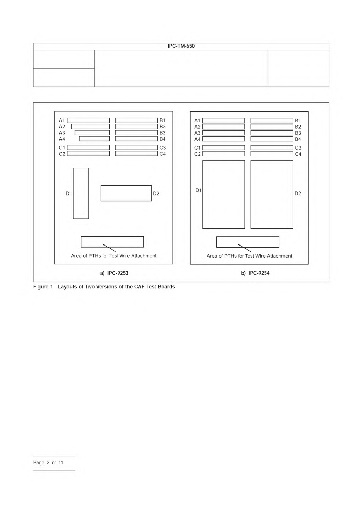
3.1 CAF Test Board Designs
The IPC-9253 and IPC-
9254 have 10 layers and dimensions are approximately
125x175 mm [nominally 5x7 in]. Test board designs for evalu-
ating CAF resistance
have varying drilled hole wall to
drilled hole wall distances for plated holes. These distances
can range from as low as 0.15 mm [0.00591 in] separation for
alternate laminate materials expected to have very high CAF
resistance and minimal copper wicking out from the plated-
through hole (PTH), to as high as 0.89 mm [0.0350 in] sepa-
ration for evaluating press-fit connector applications. The
drilled hole size, rather than the finished hole size, is specified
in the chart on the bare board fabrication drawing to ensure
consistent spacing. Internal layer thieving may be added to
plane layers around the perimeter. Test boards should be
manufactured so that the machine/grain direction of the
woven fiber reinforcement is perpendicular to the rows of
same-net daisy chain vias for A1-A4 (machine/grain direction
tends to fail first). Test board designs
have sufficient
minimum spacings on outer layers to ensure that surface insu-
lation resistance failures do not occur. Layouts of the IPC-
9253 and IPC-9254 test board structures (CAF Test Boards)
are shown in Figure 1.
3000 Lakeside Drive, Suite 105N
Bannockburn, IL 60015-1249
IPC-TM-650
TEST METHODS MANUAL
Number
2.6.25
Subject
Conductive Anodic Filament (CAF) Resistance Test:
X-Y Axis
Date
02/21
Revision
C
Originating Task Group
Electrochemical Migration Task Group (5-32e)
C/PC@
BUILD
ELECTRONICS
IPC-TM-650
Test
Methods
Warning
1:
ASTM
D-257
Warning
2:
IPC-9253
IPC-9254
IPC-9255
IPC-9256
IPC-9691
IPC
J-STD-001
IPC
J-STD-004
IPC
J-STD-006
shall
shall
Material
in
this
Test
Methods
Manual
was
voluntarily
established
by
Technical
Committees
of
IPC.
This
material
is
advisory
only
and
"s
use
or
adaptation
is
entirely
voluntary.
IPC
disclaims
all
liability
of
any
kind
as
to
the
use,
application,
or
adaptation
of
this
material.
Users
are
also
wholly
responsible
for
protecting
themselves
against
all
claims
or
liabilities
for
patent
infringement.
Equipment
referenced
/s
for
the
convenience
of
the
user
and
does
not
imply
endorsement
by
IPC.
Page
1
of
11
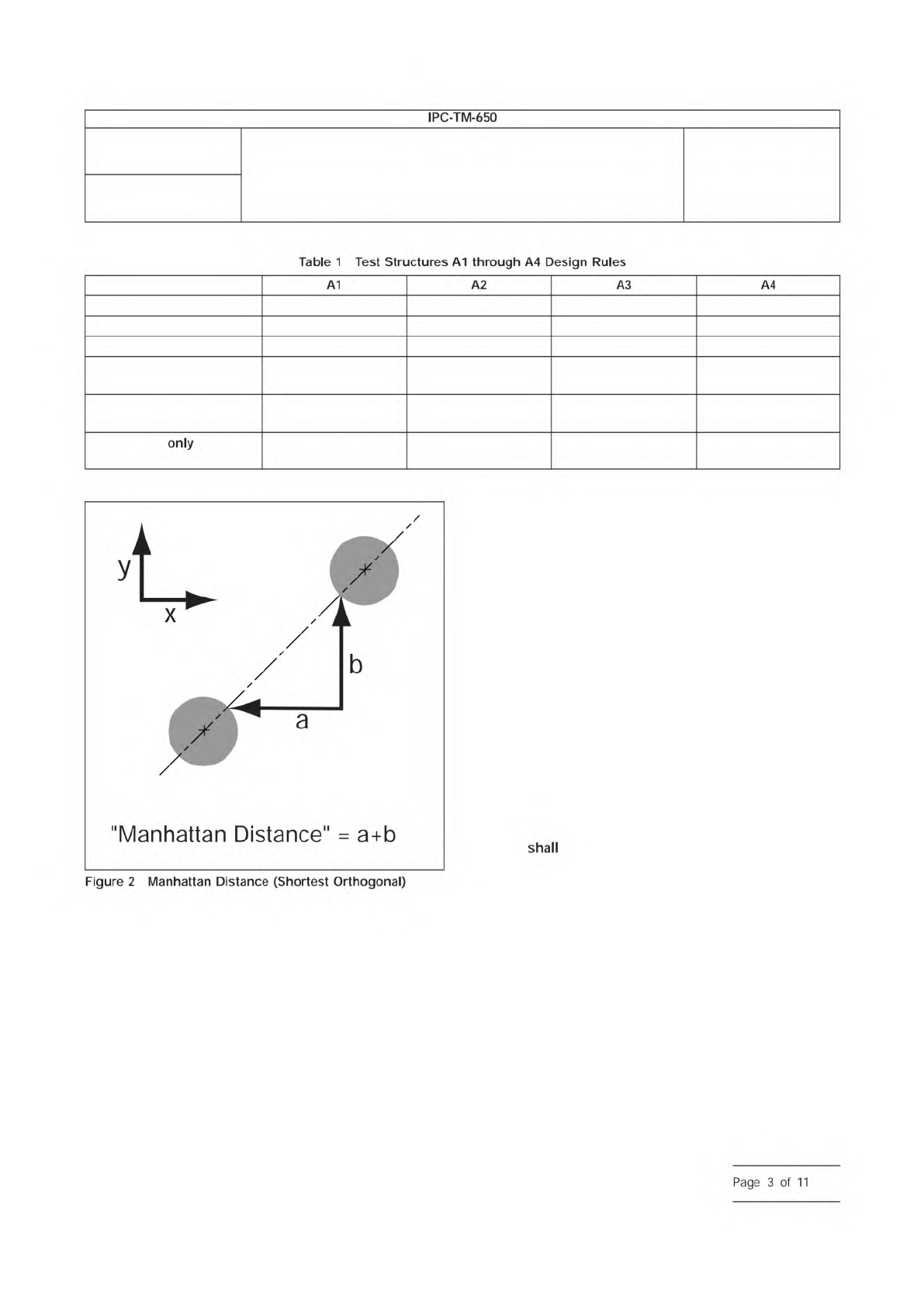
IPC-9253 and IPC-9254 Test Structures A1 through A4
The four structures A1-A4 each have five rows of connected
vias. Within each structure each row has 42 vias with alternat-
ing rows being tied to positive or negative electrodes. The via
edge to via edge spacing is varied from one structure to the
next by using a different drilled hole size on the same 1 mm
[0.040 in] pitch between rows of daisy chain vias. The result-
ing via edge to via edge spacings are: 0.27 mm, 0.38 mm,
0.51 mm, 0.65 mm [0.0106 in, 0.0150 in, 0.0201in, 0.0256
in]. Other than the use of different drilled hole sizes and a small
change in pad sizes, the four structures are identical. The vias
in these four test structures A1-A4 are aligned with the glass
fibers. Since A1-A4 evaluate susceptibility to CAF in just one
direction, test coupons should be manufactured so that the
machine direction of the woven fiber laminate reinforcement is
perpendicular to the rows of same-net daisy chain vias
(machine direction tends to fail first).
For both A and B test structures the inner and outer layer
pads are the same, i.e., the same pad size is consistently
used within a given test structure, although it does change
from structure to structure. All via to electrode connections
are made on layer 2 and are repeated on layer 9 so that a
single etch-out will not affect results. Traces from via to elec-
trode are routed on internal layers rather than external layers
to minimize potential for surface insulation resistance failure.
Design details for each test structure A1-A4 follows in Table 1.
Note: ‘‘Manhattan Distance’’ is the shortest orthogonal
distance along the X- and/or Y- axes lines between adjacent
drilled hole features (corresponds to the orthogonal nature
of the laminate material’s woven glass fiber reinforcement
(Figure 2).
IPC-9253 and IPC-9254 Test Structures B1 through B4
The four ‘‘B’’ test structures have seven alternating rows of
vias. Within each structure, alternating rows have either 27 or
26 vias with the alternating rows being tied to either positive
or negative electrodes. The via edge to via edge spacing is
varied from one structure to the next by using a different
drilled hole size on the same 1.52 mm x 1.52 mm [0.05984 in
x 0.05984 in] via grid. The 1.52 mm x 1.52 mm [0.05984 in x
0.05984 in] grid has an interstitial via therefore, tipping at a
IPC-2625-1
Number
2.6.25
Subject
Conductive Anodic Filament (CAF) Resistance Test: X-Y Axis
Date
02/21
Revision
C
IPC-TM-650
—
b)
IPC-9254
A1
B1
A2
B2
A3
B3
A4
B4
C1
C3
C2
C4
D1
D2
Area
of
PTHs
for
Test
Wire
Attachment
Figure
1
Layouts
of
Two
Versions
of
the
CAF
Test
Boards
Page
2
of
11
45° angle results in a square 1.08 mm x 1.08 mm [0.04252 in
x 0.04252 in] grid. Note: the sketches do not look square
when tipped 45° but, the CAF Test Boards do. The resulting
via edge to via edge spacings are: 0.26 mm, 0.37 mm,
0.51 mm, 0.62 mm [0.0102 in, 0.0146 in, 0.0201 in,
0.0244 in]. Other than the use of different drilled hole sizes
and a small change in pad sizes, the four structures are iden-
tical. The vias in the ‘‘B’’ test structure are not aligned with the
glass fibers. If the failure mode is along glass bundles it is rea-
sonable to expect the ‘‘B’’ test structure to perform better
than the ‘‘A’’ structure for equivalent via edge to via edge
spacings. Within a given test structure, the inner and outer
layer pads for all 10 layers are the same, i.e., the same pad
size is consistently used within a given test structure although,
it does change from structure to structure. All via to electrode
connections are made on layer 1 and are repeated on layer 10
so that a single etch-out will not affect results.
A conceptual representation of the ‘‘B’’ test structure of
the coupons in Figure 1 is shown to the upper right.
Design details on each of the four ‘‘B’’ test structures follows
in Table 2.
3.2 Other Structures
Section C is designed to evaluate
plated-through hole (PTH)-to-plane layer spacings. It is rec-
ommended to use the registration coupon per test board (IPC
Test Pattern F) when CAF testing includes this region. Section
D in the IPC-9254 design is for layer-to-layer Z-axis CAF test-
ing. Section D in the IPC-9253 is for evaluating CAF resis-
tance in a press-fit compliant pin connector application. The
feature in the D region is an optional feature that is present
automatically with the design. However, the A, B and C
regions
remain as designed in order to provide a stan-
dard basis of comparison.
The CAF test board with 10 layers is designated to evaluate
thin single-ply constructions typically used on high perfor-
mance boards. This board construction stackup can be
reduced down to: (a) four layers by eliminating layers 3
through 8 and (b) only test structures A and B, when just
evaluating differences between laminate materials.
3.3 CAF Test Board Design
This 10-layer CAF test board
for evaluating the insulation resistance between internal con-
ductors within a printed wiring board has the following key
features for evaluating hole-hole CAF resistance (Figure 3).
Holes In-Line (in-line with glass fiber direction): There are two
rows of 42 signal-1 vias intermeshed with three rows of 42
Outer layer pad size 0.86 mm [0.0339 in] 0.81 mm [0.0319 in] 0.75 mm [0.0295 in] 0.69 mm [0.0272 in]
Inner layer pad size 0.86 mm [0.0339 in] 0.81 mm [0.0319 in] 0.75 mm [0.0295 in] 0.69 mm [0.0272 in]
Drilled hole size 0.74 mm [0.0291 in] 0.63 mm [0.0248 in] 0.51 mm [0.0201 in] 0.37 mm [0.0146 in]
Via edge to via edge
(shortest distance)
0.27 mm [0.0106 in] 0.38 mm [0.0150 in] 0.51 mm [0.0201 in] 0.65 mm [0.0256 in]
Via edge to via edge
(Manhattan Distance)
0.27 mm [0.0106 in] 0.38 mm [0.0150 in] 0.51 mm [0.0201 in] 0.65 mm [0.0256 in]
On IPC-9254
, bias
applied between:
J1, J5 J2, J5 J3, J5 J4, J5
IPC-2625-2
Number
2.6.25
Subject
Conductive Anodic Filament (CAF) Resistance Test: X-Y Axis
Date
02/21
Revision
C
IPC-TM-650
—
Table
1
Test
Structures
A1
through
A4
Design
Rules
A1
A2
A3
A4
only
"Manhattan
Distance"
=
a+b
Figure
2
Manhattan
Distance
(Shortest
Orthogonal)
shall
Page
3
of
11