IPC-TM-650 EN 2022 试验方法--.pdf - 第744页
Figure 3 Four Probe Interconnect R esistance Measurement T echn ique f or Flex to PWB and Flex to ITO Glass VI Ih, Vh I1 R1= AV/I 6th tra ce Figure 2 Interconnection Resi stan ce T es t Assembly; Flex to PWB 0.4 mm Flex,…
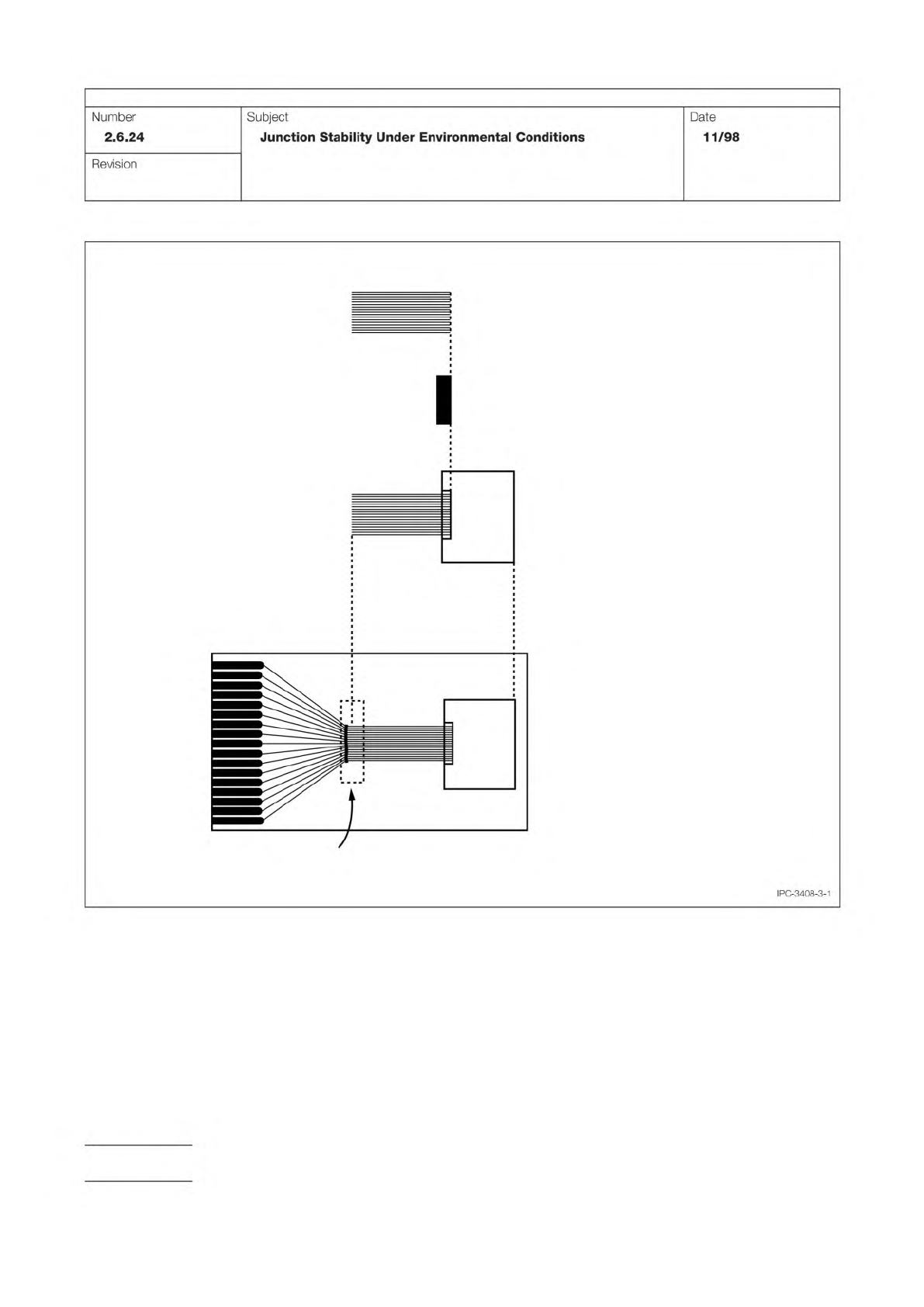
Figure 1 Interconnection Resistance Test Assembly; Flex to ITO Glass
0.4 mm Flex, 9 x 25 mm
9.0 mm x 2.5 mm nom.
ZAF, 0.025 mm, 3.2 x 10 mm
Bonded Test Sample
0.2 mm line/space
Pitch Flex-ITO Glass
Test Sample Clamped
to 0.4 mm Pitch Test Board
Clamp
IPC-TM-650
Page 2 of 3
Number
2.6.24
Subject
Junction
Stability
Under
Environmental
Conditions
Date
11/98
Revision
IPC-3408-3-1
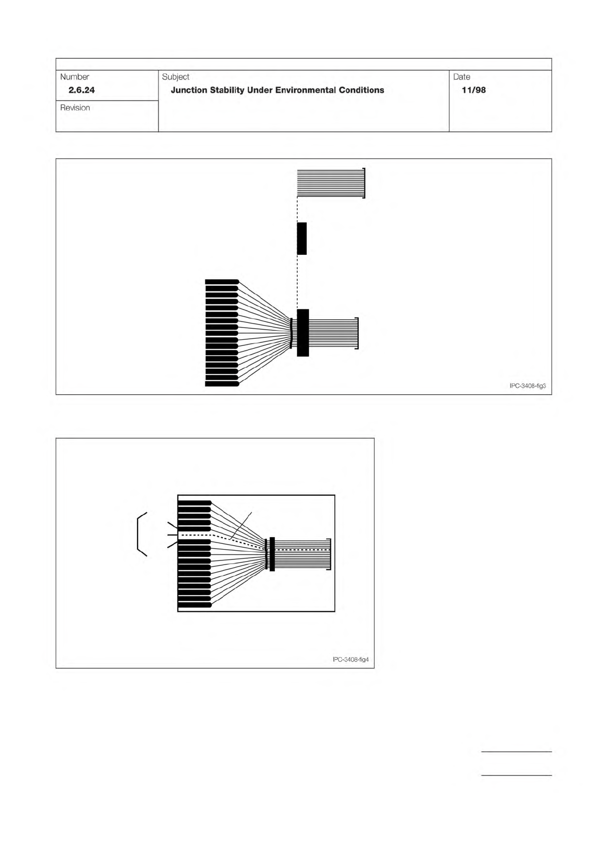
Figure 3 Four Probe Interconnect Resistance Measurement Technique for
Flex to PWB and Flex to ITO Glass
VI
Ih, Vh
I1
R1= AV/I
6th trace
Figure 2 Interconnection Resistance Test Assembly; Flex to PWB
0.4 mm Flex, Shortened on End
17 Traces, 9 mm x 25 mm
ZAF, 0.050 mm, 3.2 mm x 10 mm
Bonded Test Sample
0.2 mm line/space
Pitch Flex Board
IPC-TM-650
Page 3 of 3
Number
2.6.24
Subject
Junction
Stability
Under
Environmental
Conditions
Date
11/98
Revision
IPC-3408-fig3
IPC-3408-fig4
1 Scope
This test method provides a means to assess the propensity
for conductive anodic filament (CAF) growth and other forms
of electrochemical migration failure modes within a printed
board (PB). This test method can be used to assess PB lami-
nate materials, PB design and application parameters, PB
manufacturing process changes and other applications such
as press-fit connectors.
This IPC test method has not been designed for
use with voltages exceeding 100 Vdc bias, however higher
voltage bias testing is being routinely required to be per-
formed, such as for electric vehicle electronics. Note that at
100 Vdc using 20 mA cut-off means 2 watts of power being
dissipated per channel, so using a much lower cut-off current
is recommended for better root cause failure analysis.
As voltage bias is increased, the wiring insulation
required needs to change in order to ensure operator safety.
2 Applicable Documents
2.1 IPC
CAF Test Board Design (Available in the ‘‘Drafts’’
section of the 5-32e Task Group Home Page)
CAF Test Board Design (Available in the ‘‘Drafts’’
section of the 5-32e Task Group Home Page)
CAF Test Board Design (Available in Free Down-
loads in IPC Home Page)
CAF Test Board Design (Available in Free Down-
loads in IPC Home Page)
CAF Test Method User Guide for the IPC-TM-650,
Method 2.6.25
Requirements for Soldered Electrical and
Electronic Assemblies
Requirements for Soldering Fluxes
Requirements for Electronic Grade Solder
Alloys and Fluxed and Non-Fluxed Solid Solders for Electronic
Soldering Applications
2.3.25 Detection and Measurement of Ionizable Surface
Contaminants by Resistivity of Solvent Extract
2.6.27 Thermal Stress, Convection Reflow Assembly
Simulation
2.2 American Society for Testing and Materials (ASTM)
Standard Test Methods for DC Resistance or
Conductance of Insulating Materials
3 Test Specimens
The IPC-9254 CAF test board design is the older coupon and
has been superseded by the IPC-9253. The new smaller CAF
test coupons are IPC-9255 and IPC-9256 and are used for
evaluating PTH-PTH spacings only. These smaller CAF test
coupons allow users to put a CAF test coupon at the perim-
eter of their panels for testing. All IPC CAF test coupon design
Gerber files are down-loadable and are available on the IPC
committee and free download web sites.
3.1 CAF Test Board Designs
The IPC-9253 and IPC-
9254 have 10 layers and dimensions are approximately
125x175 mm [nominally 5x7 in]. Test board designs for evalu-
ating CAF resistance
have varying drilled hole wall to
drilled hole wall distances for plated holes. These distances
can range from as low as 0.15 mm [0.00591 in] separation for
alternate laminate materials expected to have very high CAF
resistance and minimal copper wicking out from the plated-
through hole (PTH), to as high as 0.89 mm [0.0350 in] sepa-
ration for evaluating press-fit connector applications. The
drilled hole size, rather than the finished hole size, is specified
in the chart on the bare board fabrication drawing to ensure
consistent spacing. Internal layer thieving may be added to
plane layers around the perimeter. Test boards should be
manufactured so that the machine/grain direction of the
woven fiber reinforcement is perpendicular to the rows of
same-net daisy chain vias for A1-A4 (machine/grain direction
tends to fail first). Test board designs
have sufficient
minimum spacings on outer layers to ensure that surface insu-
lation resistance failures do not occur. Layouts of the IPC-
9253 and IPC-9254 test board structures (CAF Test Boards)
are shown in Figure 1.
3000 Lakeside Drive, Suite 105N
Bannockburn, IL 60015-1249
IPC-TM-650
TEST METHODS MANUAL
Number
2.6.25
Subject
Conductive Anodic Filament (CAF) Resistance Test:
X-Y Axis
Date
02/21
Revision
C
Originating Task Group
Electrochemical Migration Task Group (5-32e)
C/PC@
BUILD
ELECTRONICS
IPC-TM-650
Test
Methods
Warning
1:
ASTM
D-257
Warning
2:
IPC-9253
IPC-9254
IPC-9255
IPC-9256
IPC-9691
IPC
J-STD-001
IPC
J-STD-004
IPC
J-STD-006
shall
shall
Material
in
this
Test
Methods
Manual
was
voluntarily
established
by
Technical
Committees
of
IPC.
This
material
is
advisory
only
and
"s
use
or
adaptation
is
entirely
voluntary.
IPC
disclaims
all
liability
of
any
kind
as
to
the
use,
application,
or
adaptation
of
this
material.
Users
are
also
wholly
responsible
for
protecting
themselves
against
all
claims
or
liabilities
for
patent
infringement.
Equipment
referenced
/s
for
the
convenience
of
the
user
and
does
not
imply
endorsement
by
IPC.
Page
1
of
11