2OM-1104-001.pdf - 第39页
T able 3B3 A through hole or a pad mark should have only one lead which is di- rected in increments of 45 . Consult our marketing department for details such as dimensions, etc. 0009-002 Chapter 1 2 16 AFU01EDTP 1.2 Oper…
(8) Fiducial Marks
P.E.C. Fiducial Marks
Material
• Copper Leaf (Au and Ni plating possible but mirror surfaces cannot be used.)
• Solder-Plated Marks (Consult our marketing department for details.)
• Solder Leveler (Consult our marketing department for details.)
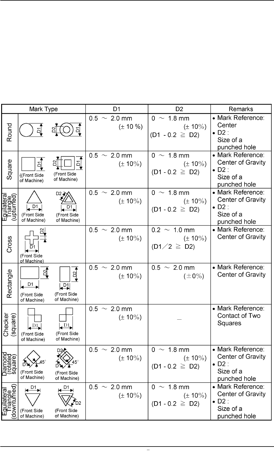
Type and Size
Table 3B2
0004-001 Chapter 1 2 15 AFU01EDTP
1.2 Operation Data
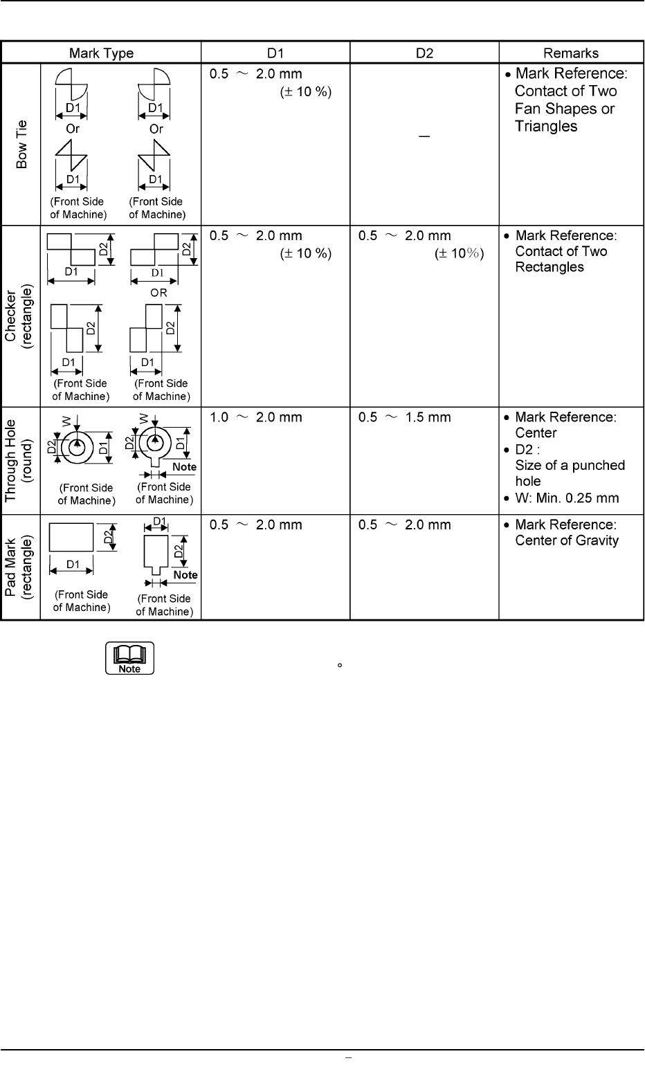
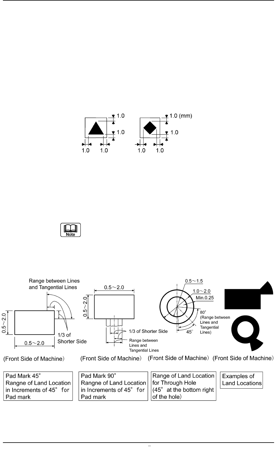
Table 3B3
A through hole or a pad mark should have only one lead which is di-
rected in increments of 45 .
Consult our marketing department for details such as dimensions, etc.
0009-002 Chapter 1 2 16 AFU01EDTP
1.2 Operation Data
Regulations regarding Mark Surroundings
• A fiducial mark should make ample contrast with the surroundings. (Preven-
tion of False Recognition)
• The shape of P.C.B. (a cutout, a punched hole), the external elements (light
reflected from a structure, light emitted from an external device, etc.,) may
sometimes interfere with recognition.
(Consult our marketing department for details.)
• A copper leaf, a resist, a coating, a silk print, and a punched hole should not
exist in the range of 1.0 mm in both X and Y directions from the outermost
edges of a fiducial mark. They may cause false recognition.
Fig. 3B50
• Anything resembling a pattern similar to a fiducial mark should not exist in
the designated recognition area. If one exists, it may cause false recogni-
tion.
Refer to "Chapter 2" in "Volume 1" for the material of the screen
plate and the settings of screen fiducial marks.
Specification of Lines extended from a Pad Mark or a Through Hole
Unit: mm
Fig. 3B52
0009-002 Chapter 1 2 17 AFU01EDTP
1.2 Operation Data