00191413-01.pdf - 第219页
User Manual Line Computer UNIX 6 Product / Package Form Software Version 501.xx 01/99 Issue 6.1 Package Form Editor 6 - 41 Allocating the new pin model to the current pin group IIf several pin mod els were alr eady defi …

6 Product / Package Form User Manual Line Computer UNIX
6.1 Package Form Editor Software Version 501.xx 01/99 Issue
6 - 40
-
Number of pins
number of pins
-
Spacing
[mm] distance between pin centers
-
Pin angle
[degree] positional angle of pins
(for component side: top 90°, bottom -90°, right 0°, left 180°)
-
X
[mm] distance between component center and center of
pin group in x-direction
-
Y
[mm] distance between component center and center of
pin group in y-direction
Procedure to be followed for editing:
●
Click on the individual editing fields and enter the values.
NOTE
Every time the RETURN key is pressed following an entry in one of the editing fields, the graphical
representation of the package form in the view area is automatically updated.
●
Confirm completion of the entries by clicking on
OK
.
The window is closed. The new group is displayed in the view area of the main window.
NOTE
If invalid values (e.g. excessive value for the number of pins) or characters (e.g. letters, or a comma as
decimal point), a dialog box containing an appropriate error message is displayed (see page 6 - 15).
The fields containing the invalid values are surrounded by a red frame.
The dialog box must be acknowledged by clicking on
OK
first. Thereafter, the entries can be correc-
ted and confirmed by clicking on
OK
.
The edited values are retained when the window is closed. If, however, no
saving procedure is car-
ried out upon exiting the Package Form Editor, the edited data will be lost.
Changing a pin group
●
Click on any pin of the desired group in the view area.
The group is identified by a rectangle surrounding it.
●
Once again select the pin by double-clicking.
The window for editing the pin group is opened (see Fig. 6.1.20).
●
Click on the editing field containing the value to be changed (cursor to be positioned in front of the
value).
●
Delete the value using the DELETE key and enter new value.
●
After all the required changes have been completed, click on
OK
.
If the values entered are valid, the window will be closed.
The pin group is displayed in the view area with the modified dimensions.
User Manual Line Computer UNIX 6 Product / Package Form
Software Version 501.xx 01/99 Issue 6.1 Package Form Editor
6 - 41
Allocating the new pin model to the current pin group
IIf several pin models were already defined, the data of the models are displayed in the "Models" selection
field (see Fig. 6.1.20) and can thus be allocated to the current pin group.
The entry for a pin model comprises the following data:
Num
= Number of the pin model
Len
= Length of the pin model
Wid
= Width of the pin model
LTo
= Length tolerance of the pin model
WTo
= Width tolerance of the pin model
CoL
= Contact length
CoW
= Contact width
Procedure:
●
Select the data of the desired pin model from the "Models" selection field.
●
Click on
OK
.
The window is closed. The pin group is displayed in the view area with the dimensions of the
selected pin model.
Defining a new pin model
●
From the view area select any pin of the newly created group by double-clicking. The window for
editing the data for the pin model is opened (see Fig. 6.1.21).
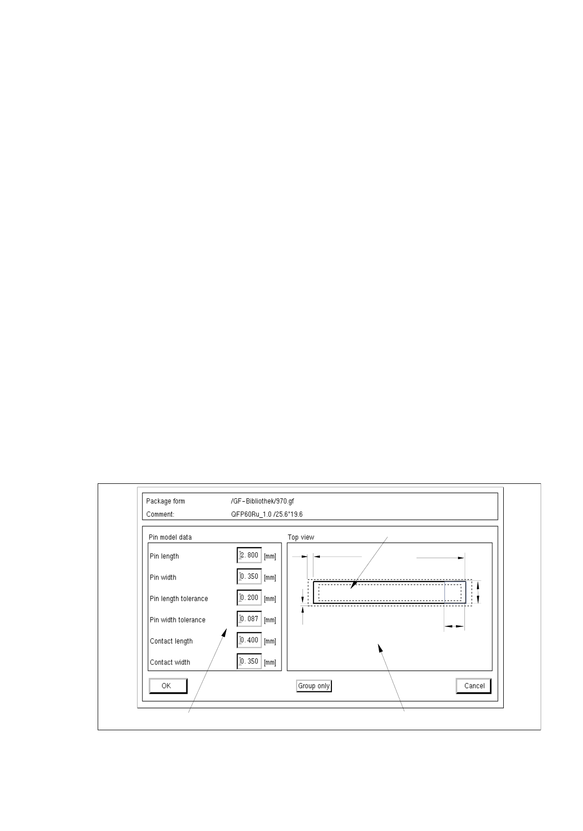
Fig. 6.1.21 Window "Model Description"
view area
editin
g
fields
pin model
Len
LTol
CoL
WTol
Wid / CoW
6 Product / Package Form User Manual Line Computer UNIX
6.1 Package Form Editor Software Version 501.xx 01/99 Issue
6 - 42
In the following, the meaning of the individual editing fields for the pin data is explained (see also
Fig. 6.1.18 and Fig. 6.1.19).
-
Pin length
[mm] length of the pin
-
Pin width
[mm] width of the pin
-
Pin length tolerance
[mm] max. permissible deviation from the pin length
-
Pin width tolerance
[mm] max. permissible deviation from the pin width
-
Contact length
[mm] length of the pin that makes contact with the PCB
-
Contact width
[mm] width of the pin that makes contact with the PCB (
^
pin width)
NOTE
From some values of the pin data the default values for the remaining pin data can be derived:
e.g. pin width (Wid) = contact width (CoW)
pin length (Len) > contact length (CoL)
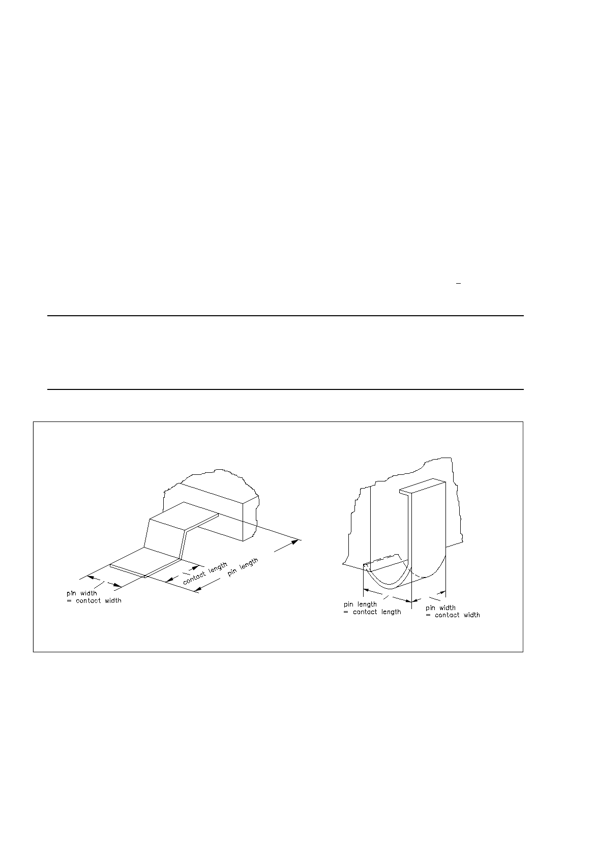
Fig. 6.1.22 Example: Pin length/Pin width