00191413-01.pdf - 第262页
8 Product / PCB User Manual Line Computer UNIX 8.1 PCB Editor Software Version 501.xx 01/99 Issue 8 - 24 Offset vector connects the zer o point of a substr ucture to the zero p oint of the super ior subst ructure an d he…

User Manual Line Computer UNIX 8 Product / PCB
Software Version 501.xx 01/99 Issue 8.1 PCB Editor
8 - 23
- cross highlighted in gray Identifies placement positions allocated to specific placement levels.
- cross highlighted in blue Identifies placement positions allocated to the currently selected place-
ment level.
- cross highlighted in Identifies placement positions allocated to the placement level that, within
light blue the placement sequence, precedes the currently selected placement level.
Meaning of the Colors in the Structure Graphic:
- black the offset data of the substructure and all of its higher-level substructures are defined.
The substructure is already displayed in the Graphic Mode.
- red the offset data of the substructure are completely defined, not however, those of all supe-
rior substructures thereof. The substructure is not displayed in the Graphic Mode yet.
- gray the offset data of the substructure have not been completely defined yet. The substructure
is not displayed yet in the Graphic Mode, and any possible display of its lower-level sub-
structures is suppressed.
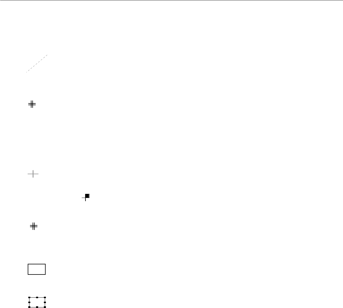
8.1.3.8 Symbols and Their Meanings in the Structure Editor (Graphic Mode)
In the Graphic Mode of the PCB Editor a series of symbols are used each of which has a different meaning.
In the following, the meaning of the symbols is explained.
Outline (dimensions) of the PCB
It is uniquely defined by the length and width of the PCB or substructure.
Name of the PCB or the PCB substructure (color blue)
<Name> The name is always displayed above the upper left corner of the outline, with the same orientation
as the substructure.
Zero point
This symbol identifies the zero point of the coordinate system of the PCB or substructure.
Coordinate system of a substructure
This graphic indicates the position of the coordinate system of the substructure.
The arrow marks the x-axis and always identifies the positive direction of the axis.
Dimensional vectors
They symbolize the two vectors from the PCB zero point to corner "1" and corner "2" of the PCB
outline (see graphical display on page 8 - 28).
8 Product / PCB User Manual Line Computer UNIX
8.1 PCB Editor Software Version 501.xx 01/99 Issue
8 - 24
Offset vector
connects the zero point of a substructure to the zero point of the superior substructure and hence
corresponds to the offset or displacement vector between the two coordinate systems of these
substructures.
PCB fiducial
This symbol indicates the position of a PCB-related fiducial.
It is always displayed in the shape of a double cross, irrespective of the actual shape of the fiducial.
Ink spot
l This symbol indicates the position of the fiducials defined as inkspots.
It is always displayed in the shape of a dot, irrespective of the actual shape of the fiducial.
Placement position (color green)
This symbol indicates the position of the placement position or the zero point of the coordinate
system of the placement position.
To identify the position of pin 1, the quadrant in which pin 1 is located is highlighted in solid color.
Example :
Placement position fiducial
This symbol indicates the position of a PP-related fiducial.
It is always displayed in the shape of a double cross, irrespective of the actual shape of the fiducial,
and it is significantly smaller than the symbol of a PCB fiducial.
Frame around a selected placement position and/or substructure
The frame marks the outline of the currently selected substructure.
The frame marks the currently selected placement position.
Frame around placement position(s) or a substructure
The frame marks the outline of a substructure which is linked to the currently selected sub-
structure.
The frame marks the placement positions which are linked to the currently selected placement
position.
User Manual Line Computer UNIX 8 Product / PCB
Software Version 501.xx 01/99 Issue 8.1 PCB Editor
8 - 25
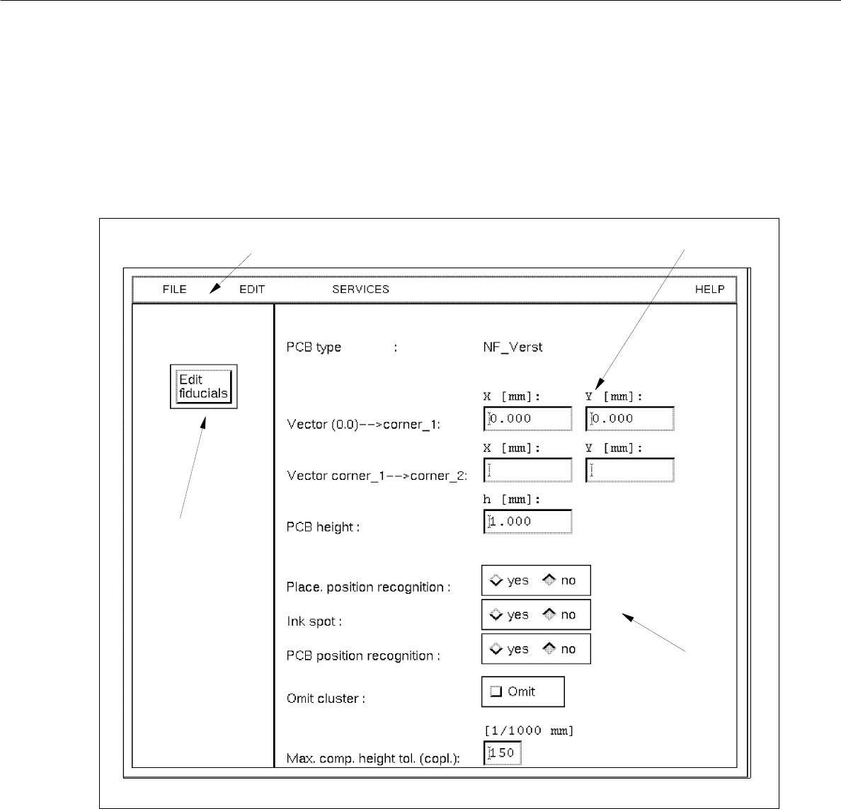
8.1.4 Cluster Editor Window
A Cluster Editor can be opened for each PCB type generated (see description on page 8 - 10).
In the following, the different areas of the Cluster Editor window and their functions are explained.
Fig. 8.1.8 Window "Cluster Editor"
The window is subdivided as follows:
- Menu bar
- Editing area
- Setting area
- Command button
menu bar
editing area
command button
setting area