00191413-01.pdf - 第547页
User Manual Line Computer UNIX 17.3 Description of Components and P CBs Software Version 501.xx 01/99 Issue 17.3.1 PCB 1: sin g le circuit 17 - 1 5 17.2.1.1 Package Form Description The packa g e forms used are c ontain …
17.3 Description of Components and PCBs User Manual Line Computer UNIX
17.3.1 PCB 1: sin
g
le circuit Software Version 501.xx 01/99 Issue
17 - 14
The packa
g
e form description is dispensed with.
The adhesive pattern description is dispensed with.
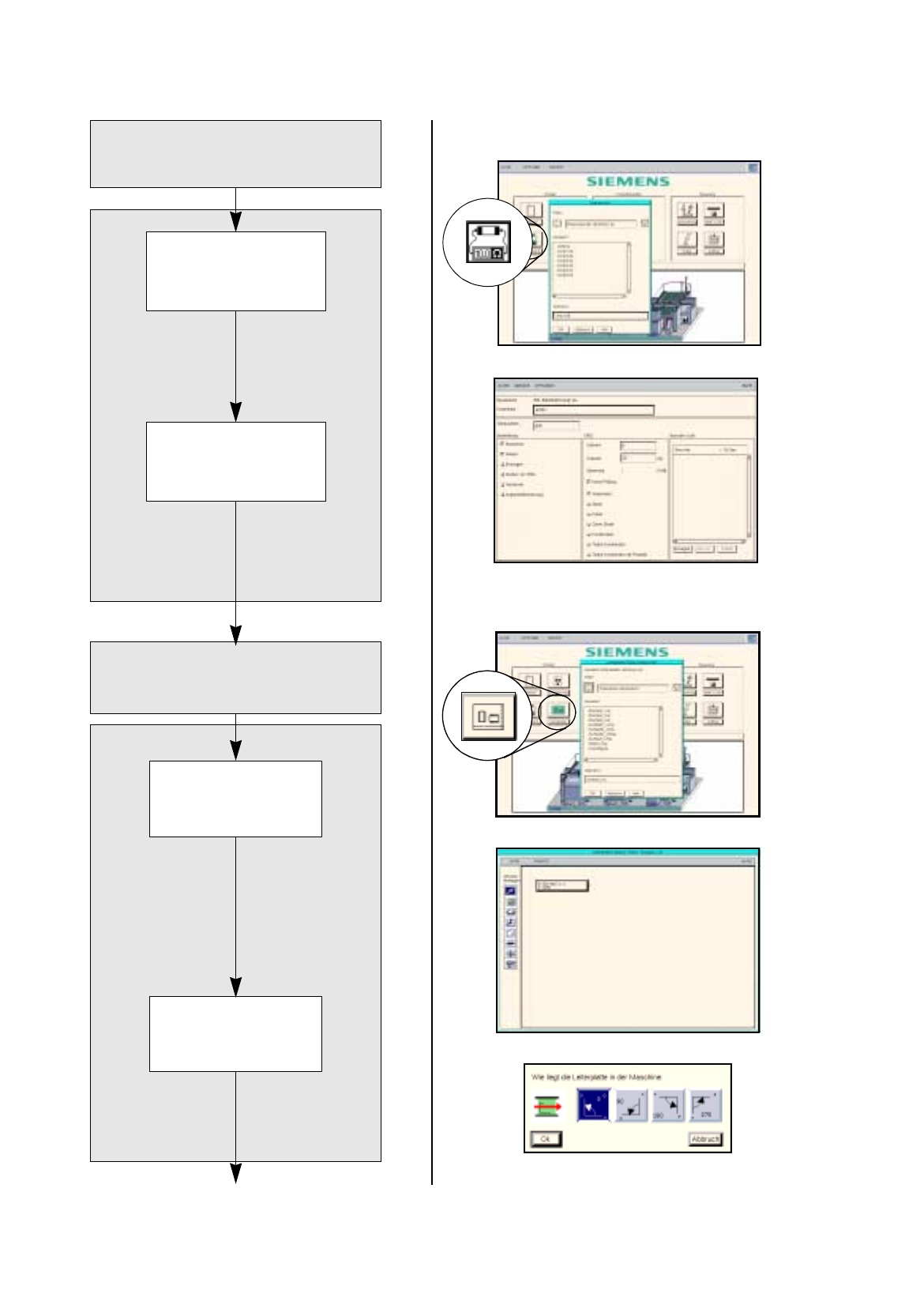
Open Component
Editor for a component
Enter component data
Component description
Adh. pattern description
Starting PCB Editor
for a PCB
Indicate position of
PCB in the machine
PCB Description
continued on pa
g
e 17-16
Packa
g
e form
description
User Manual Line Computer UNIX 17.3 Description of Components and PCBs
Software Version 501.xx 01/99 Issue 17.3.1 PCB 1: sin
g
le circuit
17 - 15
17.2.1.1 Package Form Description
The packa
g
e forms used are contained in the standard GF-librar
y
, the description is dispensed with.
17.2.1.2 Component Description
To open the Component Editor for a component, proceed as follows:
1. On the desktop click on the icon of the Component Editor .
The file selection window is opened.
2. Click on the
Selection
editin
g
field.
3. Enter the name of the component, here:
Comp1.be
, click on the
OK
button.
The Component Editor is opened.
To enter the component data, proceed as follows:
4. Click on the
Comment
editin
g
field.
5. Enter a comment uni
q
uel
y
describin
g
the component, here:
SOT23
.
6. Click on the
Package form
editin
g
field.
7. Enter the packa
g
e form number, here:
400
.
8. Activate the appropriate button in the
Processing
selection area, here:
Placing
and
Glueing
.
9. Activate the appropriate button in the CRDL selection area, here:
No check
.
10. On the
FILE
menu click on the
Save
option.
The component data are now saved.
11. On the
FILE
menu click on the
Quit
option.
The Component Editor is closed.
12. Perform the component description for the other components, here:
Comp2.be
and
Comp3.be
.
17.2.1.3 Adhesive Pattern (DM) Description
An adhesive pattern has alread
y
been defined in the standard GF-Bibliothek for the packa
g
e forms defined.
17.2.1.4 PCB Description
To open the PCB Editor for a PCB, proceed as follows:
13. On the desktop click on the icon of the PCB Editor .
The file selection window is opened.
14. Click on the
Selection
editin
g
field.
15. Enter the name of the PCB, here:
Example_1.la
and click on the
OK
button.
A dialo
g
box is opened.
16. Click on the
TYPE
editin
g
field.
17. Enter a t
y
pe desi
g
nation, here:
SMD a
nd click on the
OK
button.
The PCB Editor is opened. The PCB is represented as a rectan
g
le.
To specify the position of the PCB in the machine, proceed as follows:
18. Activate the Coordinate S
y
stem icon.
19. Click on the PCB
(
rectan
g
le
)
.
A dialo
g
box containin
g
the displa
y
of four coordinate s
y
stems is opened.
20. Click on a coordinate s
y
stem, here:
0°
.
21. Click on the
OK
button.
The dialo
g
box is closed.
17.3 Description of Components and PCBs User Manual Line Computer UNIX
17.3.1 PCB 1: sin
g
le circuit Software Version 501.xx 01/99 Issue
17 - 16
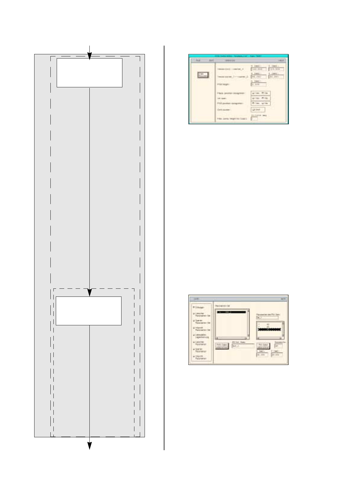
Entering the dimens-
ions of the PCB
Defining fiducials
continued from pa
g
e 17-14
PCB Description
Cluster Editor
Fiducial Editor
continued on pa
g
e 17-18