00191413-01.pdf - 第574页
17.3 Description of Components and PCBs User Manual Line Computer UNIX 17.3.3 PCB 3: Focus on Cluster Technique Software Vers ion 501.xx 01/99 Issue 17 - 42 The pack a g e form des cription is disp ensed with . The compo…
User Manual Line Computer UNIX 17.3 Description of Components and PCBs
Software Version 501.xx 01/99 Issue 17.3.3 PCB 3: Focus on Cluster Technique
17 - 41
pattern_2
pattern_1
pattern_3
pattern_4
board 1
board2
board 3
board 1
board2
board 3
board 3
board2
board 1
board 3
board2
board 1
Example_3
5
10
15
Corner
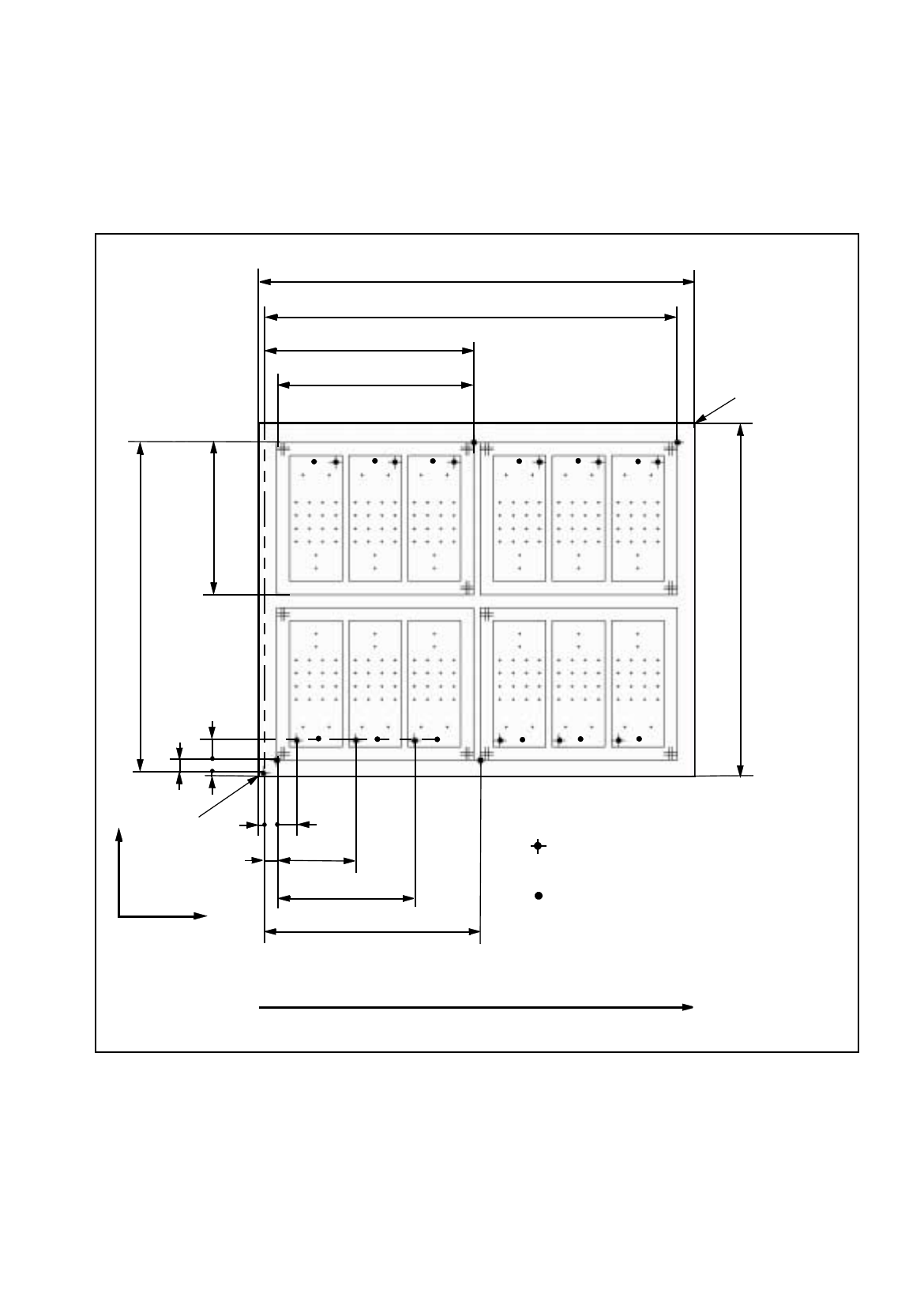
17.3.3 PCB 3: Focus on Cluster Technique
PCB 3 consists of four clusters
(
pattern
)
each of which comprises three sin
g
le circuits
(
board
)
. The dimensions
and the placement confi
g
uration of the sin
g
le circuits corresponds to those of PCB 2. Clusters 3 and 4 are ro-
tated b
y
180°. For each cluster a PCB position reco
g
nition operation is performed. Three fiducials are available
in each case. An ink spot is located on each sin
g
le circuit.
335
272
5
X
Y
PCB coordinate
system 0°
Direction of travel
150
116
10
15
60
105
165
Corner
PCB hei
g
ht= 1.5 mm
Zero point of the different levels:
PCB, cluster, sin
g
le circuit
Ink spot
Fig. 17.3.7 Dimensions PCB 3
252
160
315
17.3 Description of Components and PCBs User Manual Line Computer UNIX
17.3.3 PCB 3: Focus on Cluster Technique Software Version 501.xx 01/99 Issue
17 - 42
The packa
g
e form description is dispensed with.
The component description is dispensed with.
The adhesive pattern description is dispensed with.
No fiducials are present.
No ink spot is present.
The placement positions are defined in the
sin
g
le circuits.
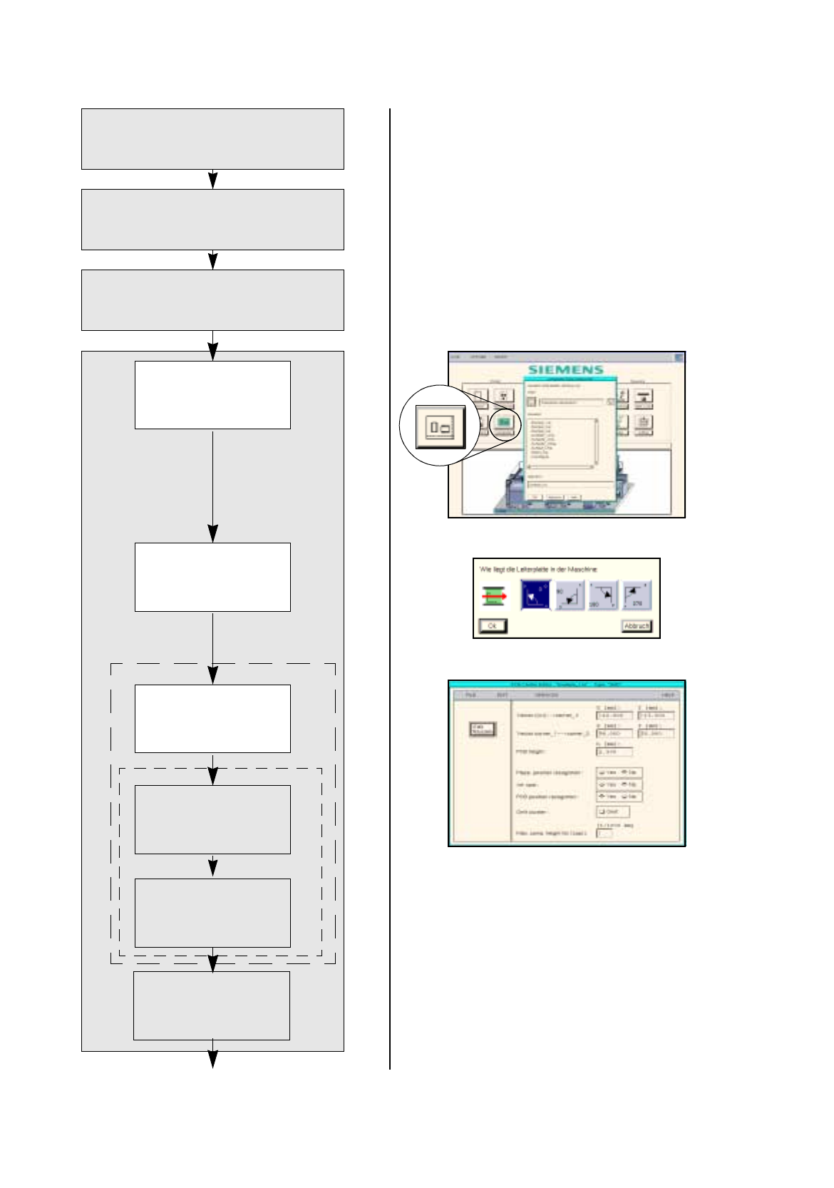
Pack. form description
Starting the PCB
Editor for a PCB
Indicating position of
PCB in the machine
Defining ink spot
Component description
Adh. pattern description
Entering dimensions
of PCB
Defining fiducials
continued on pa
g
e 17-44
Cluster Editor
Fiducial Editor
Entering placement
positions
PCB description
User Manual Line Computer UNIX 17.3 Description of Components and PCBs
Software Version 501.xx 01/99 Issue 17.3.3 PCB 3: Focus on Cluster Technique
17 - 43
17.2.3.1 Package form description
PCB 3 consists of four clusters with three sin
g
le circuits each, all of which correspond to PCB 2.
For the packa
g
e form description refer to section 17.2.2.1
17.2.3.2 Component description
PCB 3 consists of four clusters with three sin
g
le circuits each, all of which correspond to PCB 2.
For the component description refer to section 17.2.2.2
17.2.3.3 Adhesive pattern description
PCB 3 consists of four clusters with three sin
g
le circuits each, all of which correspond to PCB 2.
For the adhesive pattern description refer to section 17.2.2.3.
17.2.3.4 PCB description
The offset values are to be determined automaticall
y
from Fi
g
. 17.3.7 on pa
g
e 17-41
(
solution on pa
g
e 17-51
)
.
To open the PCB Editor for a PCB, proceed as follows:
1. On the desktop click on the icon the PCB Editor .
The file selection window is opened.
2. Click on the
Selection
editin
g
field.
3. Enter the name of the PCB
,
here:
Example_3.la,
and click on the
OK
button.
A dialo
g
box is opened.
4. Click on the
TYPE
editin
g
field.
5. Enter a t
y
pe desi
g
nation, here:
Typ_1,
and click on the
OK
button:
The Component Editor is opened. The PCB is displa
y
ed as a rectan
g
le.
To specify the position of the PCB in the machine:
6. Activate the Coordinate s
y
stem icon .
7. Click on the PCB
(
rectan
g
le
)
.
A dialo
g
box containin
g
the displa
y
of four coordinate s
y
stems is opened.
8. Click on a coordinate s
y
stem, here:
0°
.
9. Click on the
OK
button.
The dialo
g
box is closed.
To enter the dimensions of the PCB, proceed as follows:
10. Activate the Select icon .
11. Click on the PCB
(
rectan
g
le
)
.
The rectan
g
le is hi
g
hli
g
hted in
g
reen.
12. Click on the
Cluster Editor...
option on the
SERVICES
menu.
The Cluster Editor is opened.
13. Enter the dimensions of the PCB, see Fi
g
. 17.3.7 on pa
g
e 17-41.
14. Click on the
Quit
option on the
FILE
menu.
The Cluster Editor is closed.
Defining fiducials:
no fiducials are present.
Defining ink spot:
no ink spot is present.
Entering placement positions:
the placement positions are defined at a later point in the sin
g
le circuits.