00191413-01.pdf - 第546页
17.3 Description of Components and PCBs User Manual Line Computer UNIX 17.3.1 PCB 1: sin g le circuit Software Version 501.xx 01/99 Issue 17 - 14 The pack a g e form des cription is disp ensed with . The adhesi ve pa tte…
User Manual Line Computer UNIX 17.3 Description of Components and PCBs
Software Version 501.xx 01/99 Issue 17.3.1 PCB 1: sin
g
le circuit
17 - 13
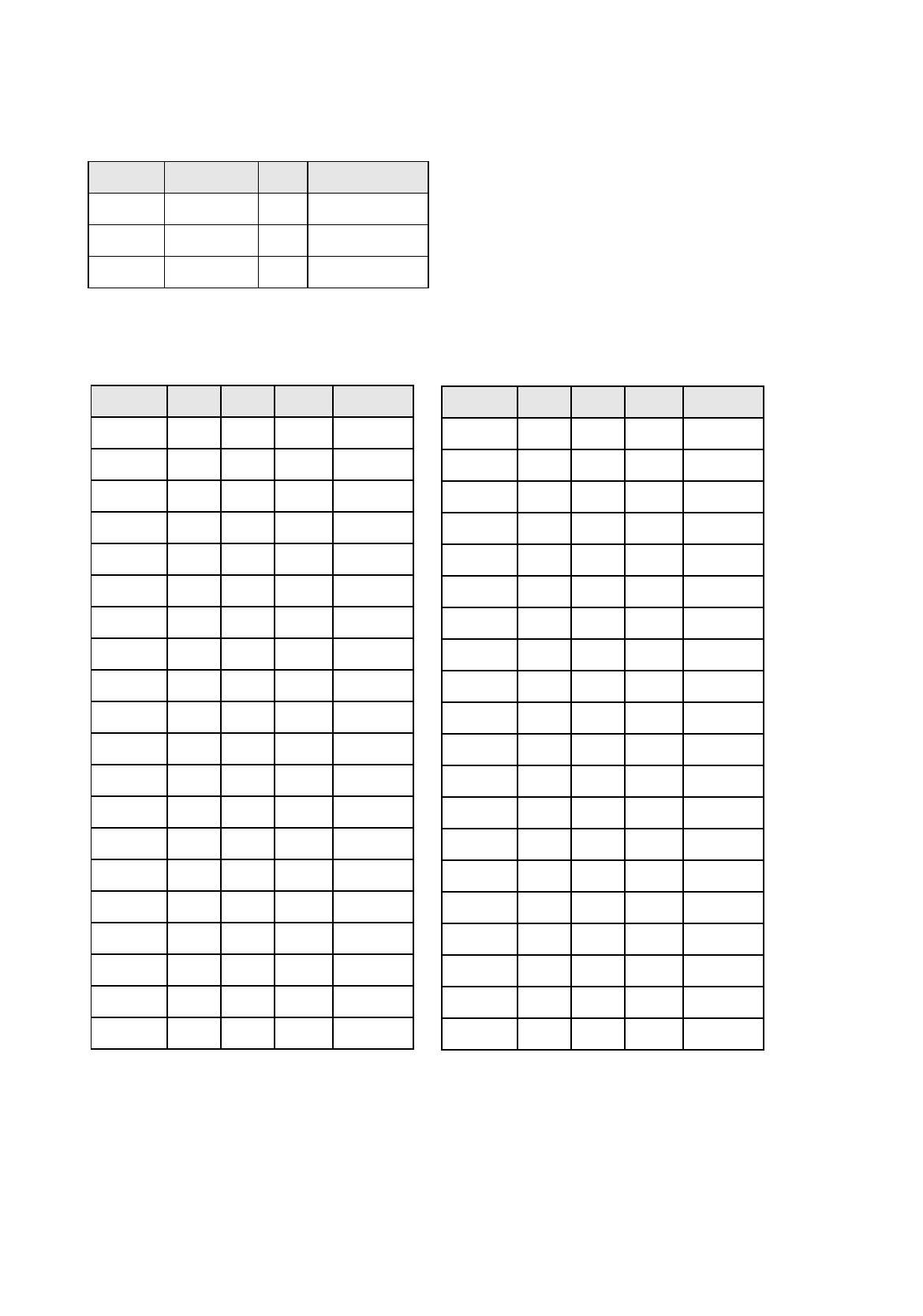
Tab. 17.3-1: Component Data PCB 1
Name Package form GF-No. Handling
Comp1.be SOT23 400 Gluein
g
, Placin
g
Comp2.be 1206 105 Gluein
g
, Placin
g
Comp3.be 0805 103 Gluein
g
, Placin
g
Comp.name X Y Angle Comment
Comp1 6.60 3.84 57.00 Pos1
Comp1 10.92 0.79 10.00 Pos2
Comp1 16.26 1.30 337.00 Pos3
Comp1 20.32 4.85 276.00 Pos4
Comp1 18.29 8.92 37.00 Pos5
Comp1 13.72 10.95 22.00 Pos6
Comp1 8.64 12.98 28.00 Pos7
Comp1 5.59 17.05 94.00 Pos8
Comp1 9.40 20.60 161.00 Pos9
Comp1 14.99 21.11 190.00 Pos10
Comp1 19.05 18.32 249.00 Pos11
Comp2 28.70 0.54 270.00 Pos14
Comp2 28.70 5.62 270.00 Pos15
Comp2 28.70 10.70 270.00 Pos16
Comp2 28.70 15.78 270.00 Pos17
Comp2 30.73 20.35 180.00 Pos18
Comp2 33.27 15.78 253.00 Pos19
Comp2 34.77 10.92 253.00 Pos20
Comp2 36.24 6.06 253.00 Pos21
Comp2 38.35 1.04 270.00 Pos22
Comp2 40.80 6.11 288.00 Pos23
Comp2 42.37 10.95 288.00 Pos24
Comp2 43.94 15.78 288.00 Pos25
Comp2 46.48 20.35 180.00 Pos26
Comp2 49.02 15.78 270.00 Pos27
Comp2 49.02 10.70 270.00 Pos28
Comp2 49.02 5.62 270.00 Pos29
Comp2 49.02 0.54 270.00 Pos30
Comp3 58.17 0.54 180.00 Pos31
Comp3 58.17 5.62 270.00 Pos32
Comp3 58.17 10.70 270.00 Pos33
Comp3 58.17 15.78 270.00 Pos34
Comp3 58.17 20.86 180.00 Pos35
Comp3 63.25 20.86 180.00 Pos36
Comp3 68.33 19.49 210.00 Pos37
Comp3 72.04 15.78 240.00 Pos38
Comp3 73.41 10.70 270.00 Pos39
Comp3 72.04 5.62 300.00 Pos40
Comp3 68.33 1.90 330.00 Pos41
Comp3 63.25 0.54 180.00 Pos42
Comp.name X Y Angle Comment
Tab. 17.3-2 Placement Positions PCB 1
17.3 Description of Components and PCBs User Manual Line Computer UNIX
17.3.1 PCB 1: sin
g
le circuit Software Version 501.xx 01/99 Issue
17 - 14
The packa
g
e form description is dispensed with.
The adhesive pattern description is dispensed with.
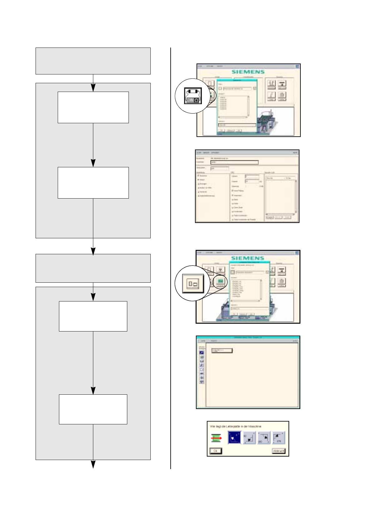
Open Component
Editor for a component
Enter component data
Component description
Adh. pattern description
Starting PCB Editor
for a PCB
Indicate position of
PCB in the machine
PCB Description
continued on pa
g
e 17-16
Packa
g
e form
description
User Manual Line Computer UNIX 17.3 Description of Components and PCBs
Software Version 501.xx 01/99 Issue 17.3.1 PCB 1: sin
g
le circuit
17 - 15
17.2.1.1 Package Form Description
The packa
g
e forms used are contained in the standard GF-librar
y
, the description is dispensed with.
17.2.1.2 Component Description
To open the Component Editor for a component, proceed as follows:
1. On the desktop click on the icon of the Component Editor .
The file selection window is opened.
2. Click on the
Selection
editin
g
field.
3. Enter the name of the component, here:
Comp1.be
, click on the
OK
button.
The Component Editor is opened.
To enter the component data, proceed as follows:
4. Click on the
Comment
editin
g
field.
5. Enter a comment uni
q
uel
y
describin
g
the component, here:
SOT23
.
6. Click on the
Package form
editin
g
field.
7. Enter the packa
g
e form number, here:
400
.
8. Activate the appropriate button in the
Processing
selection area, here:
Placing
and
Glueing
.
9. Activate the appropriate button in the CRDL selection area, here:
No check
.
10. On the
FILE
menu click on the
Save
option.
The component data are now saved.
11. On the
FILE
menu click on the
Quit
option.
The Component Editor is closed.
12. Perform the component description for the other components, here:
Comp2.be
and
Comp3.be
.
17.2.1.3 Adhesive Pattern (DM) Description
An adhesive pattern has alread
y
been defined in the standard GF-Bibliothek for the packa
g
e forms defined.
17.2.1.4 PCB Description
To open the PCB Editor for a PCB, proceed as follows:
13. On the desktop click on the icon of the PCB Editor .
The file selection window is opened.
14. Click on the
Selection
editin
g
field.
15. Enter the name of the PCB, here:
Example_1.la
and click on the
OK
button.
A dialo
g
box is opened.
16. Click on the
TYPE
editin
g
field.
17. Enter a t
y
pe desi
g
nation, here:
SMD a
nd click on the
OK
button.
The PCB Editor is opened. The PCB is represented as a rectan
g
le.
To specify the position of the PCB in the machine, proceed as follows:
18. Activate the Coordinate S
y
stem icon.
19. Click on the PCB
(
rectan
g
le
)
.
A dialo
g
box containin
g
the displa
y
of four coordinate s
y
stems is opened.
20. Click on a coordinate s
y
stem, here:
0°
.
21. Click on the
OK
button.
The dialo
g
box is closed.