00191413-01.pdf - 第251页
User Manual Line Computer UNIX 8 Product / PCB Software Version 501.xx 01/99 Issue 8.1 PCB Editor 8 - 13 - Setting cluster offset For each partial str ucture a cl uster offs et must be entered. B y entering the cluster o…
8 Product / PCB User Manual Line Computer UNIX
8.1 PCB Editor Software Version 501.xx 01/99 Issue
8 - 12
- Selection
If this icon is active (displayed in reverse video, with the arrow pointing from the bottom left to the top
right), the PP or NU-Editor can be called up for the selected partial PCB structure. If the topmost par-
tial PCB structure is selected, the current PCB can be duplicated using the "Copy PCB" menu
function.
● Activate icon .
● The partial structure selected is highlighted in light green. All partial structures linked to it are
highlighted in dark green.
● Select desired menu function (e.g. SERVICES --> NU-Editor...).
- Generating a new partial PCB structure with the corresponding new PCB type
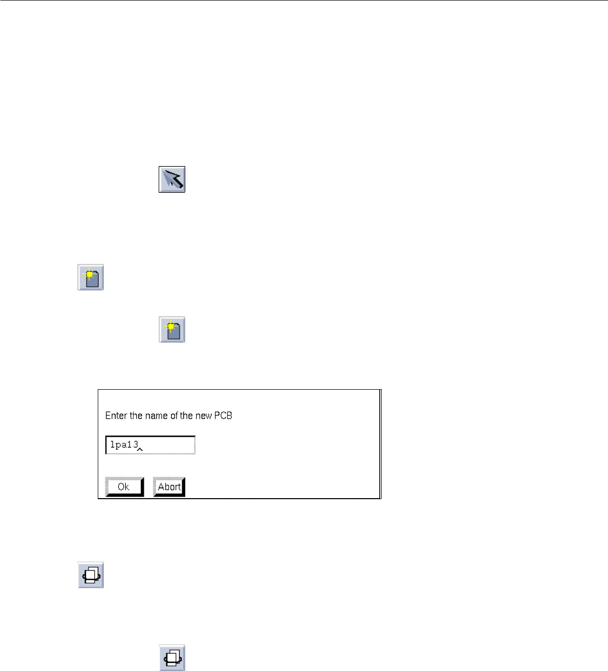
This command serves to generate a new partial structure with a cross-reference to a new PCB type.
● Activate icon .
● Select PCB type.
The following dialog box for entering the name is displayed.
● Enter the name and confirm with OK.
The new PCB type is appended to the selected one and displayed in the display area.
- Duplicating a partial PCB structure
Existing cross-references to a given PCB type can be duplicated from a PCB partial structure thus
generating a new partial structure. Except for the coordinates, the data of the duplicated partial PCB
structure are identical.
● Activate icon .
● Select partial PCB structure.
The dialog box for entering the name is displayed.
● Enter the name and confirm with OK.
User Manual Line Computer UNIX 8 Product / PCB
Software Version 501.xx 01/99 Issue 8.1 PCB Editor
8 - 13
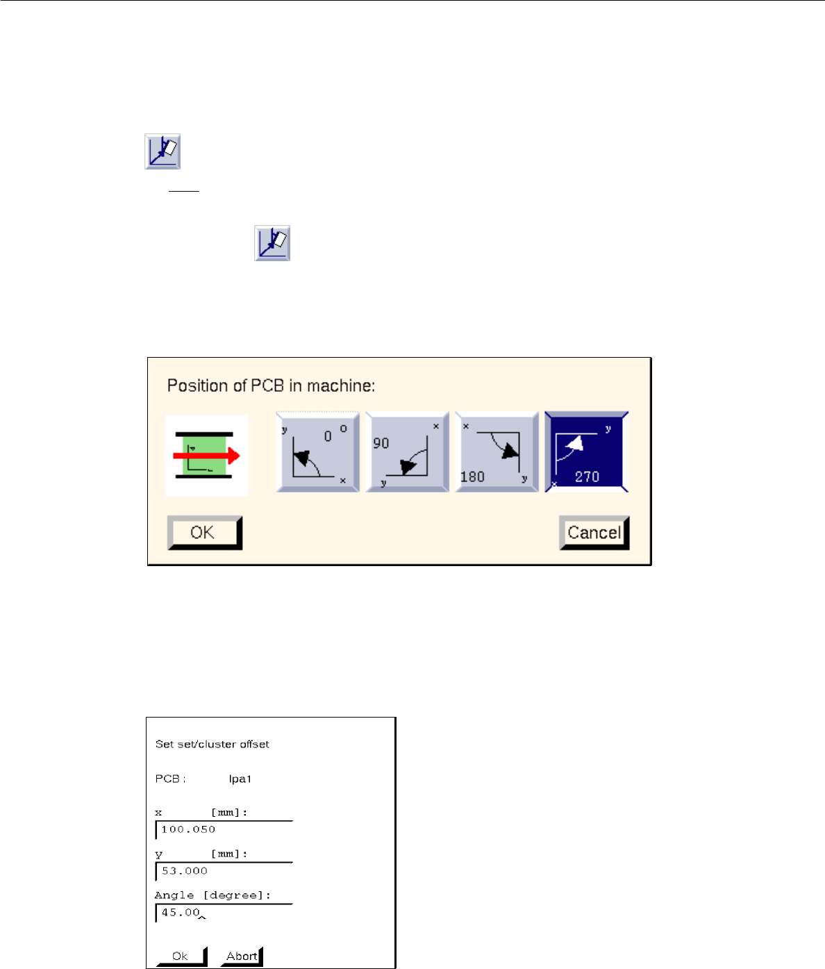
- Setting cluster offset
For each
partial structure a cluster offset must be entered. By entering the cluster offset the PCB type
is provided with a coordinate offset, and a partial PCB structure is thus completely described.
● Activate icon .
● To define the position of the board (complete cluster) in the machine, first click on the uppermost
partial PCB structure of the PCB structure.
The following dialog box appears:
● Select position by clicking on 0°, 90°, 180° or 270° in the dialog box.
● Confirm with OK.
● Click on partial PCB structure of the PCB structure.
The following dialog box appears:
● Enter x, y-coordinates and angle with respect to partial PCB structure (cluster) in which the selec-
ted lower partial structure is contained (see Fig. 8.1.2).
● Confirm with OK.
● Repeat procedure for all partial PCB structures existing in the partial PCB structures loaded.
8 Product / PCB User Manual Line Computer UNIX
8.1 PCB Editor Software Version 501.xx 01/99 Issue
8 - 14
- Copying a partial PCB structure together with the corresponding PCB type
This command serves to copy all data of the partial structure. A new partial structure containing a
cross-reference to a new PCB type is generated.
● Activate icon .
● Select PCB type in which the copied PCB type is to be contained.
● Select PCB type to be copied.
The dialog box for entering the name is displayed.
● Enter the name and confirm with OK.
Copying a partial PCB structure together with corresponding PCB type, or an overall PCB structure, into
another (loaded) PCB structure
● Activate icon .
● Load the PCB with the structure to be copied via FILE --> Open....
● In the window which is opened first click on the PCB type (target) which is to contain the copied
structure.
● Select the PCB type to be copied (source) in the second window.
● Enter name in the dialog box displayed and confirm with OK.
The copied structure is now inserted into the existing PCB structure.
- Duplicating a partial PCB structure
This command serves to generate a new partial PCB structure containing a cross-reference to a PCB
type sharing common features with other partial PCB structures. The new PCB differs from this source
PCB type only in that its coordinates are different. All other data are identical.
● Activate icon .
● Select target PCB type.
● Select source PCB type
The dialog box for entering the name is displayed.
● Enter the name and confirm with OK.