00191413-01.pdf - 第580页
17.3 Description of Components and PCBs User Manual Line Computer UNIX 17.3.3 PCB 3: Focus on Cluster Technique Software Version 501.xx 01/99 Issue 17 - 48 The definitio n of the fiducia ls is dispens ed with for the dup…

User Manual Line Computer UNIX 17.3 Description of Components and PCBs
Software Version 501.xx 01/99 Issue 17.3.3 PCB 3: Focus on Cluster Technique
17 - 47
Defining ink spot:
no ink spot is present.
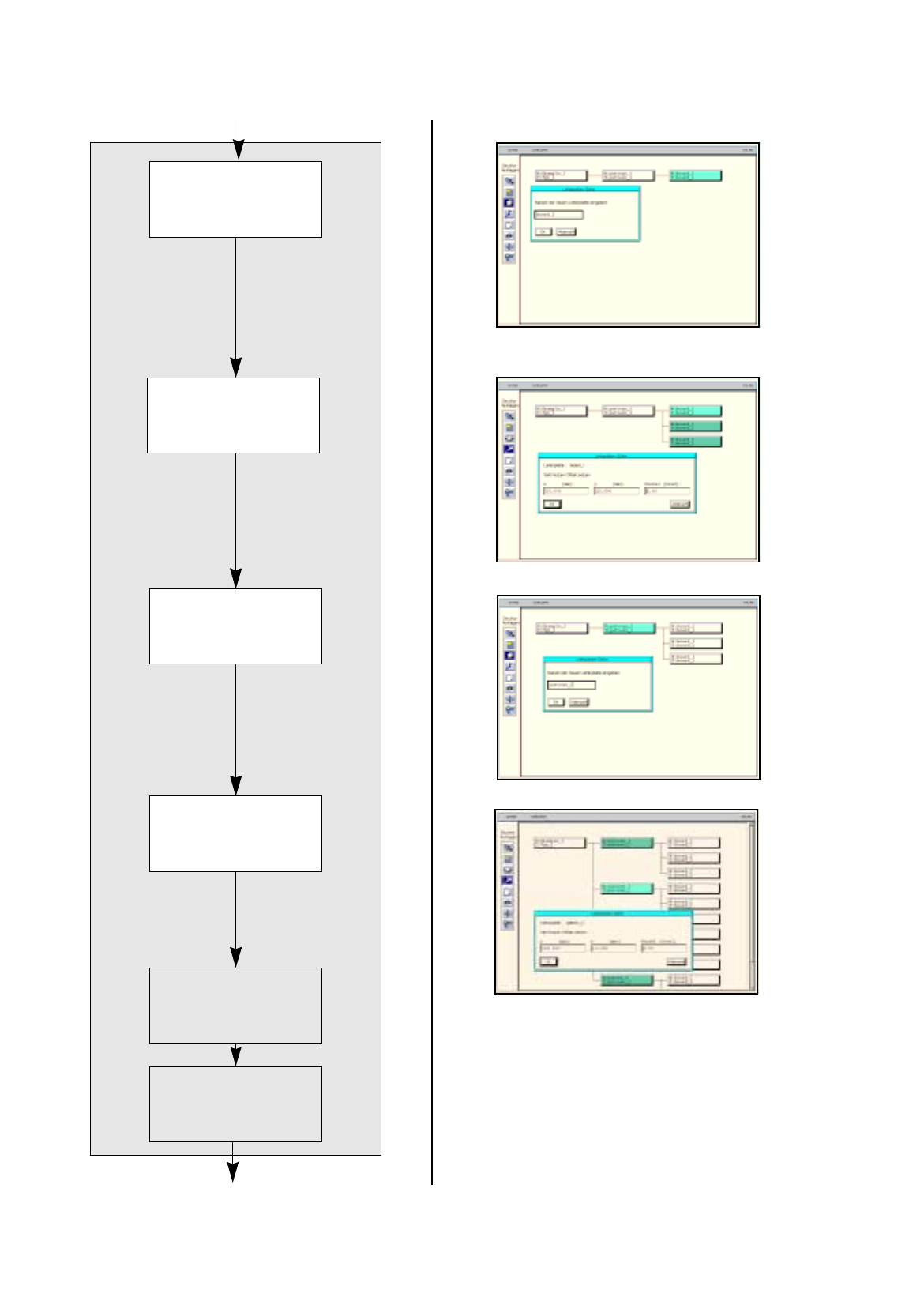
To create a single circuit in a cluster, proceed as follows:
42. Activate the Create icon .
43. Click on the cluster, here:
pattern_1
.
A dialo
g
box is opened.
44. Click on the editin
g
field.
45. Enter the name for the sin
g
le circuit, here:
board_1,
and click on the
OK
button.
The dialo
g
box is closed. The new sin
g
le circuit is displa
y
ed at the third level.
To enter the offset values for the single circuit, proceed as follows:
46. Activate the Coordinate s
y
stem icon .
47. Click on the sin
g
le circuit, here:
board_1
.
A dialo
g
box is opened.
48. Click on the individual editin
g
fields and enter the offset values, see Fi
g
. 17.3.7 on pa
g
e 17-41.
49. Click on the
OK
button.
The dialo
g
box is closed.
To load the cluster data and placement positions of another PCB for the single circuit:
50. Activate the Select icon .
51. Click on the sin
g
le circuit, here:
board_1
.
52. Click on the
Cluster Editor
option on the
SERVICES
menu.
The Cluster Editor is opened.
53. Click on the
Structure Editor
option on the
SERVICES
menu.
A file selection window is opened.
54. Select a PCB b
y
double-clickin
g
, here:
Example_2.la
.
The PCB Editor for Example_2.la is opened.
55. Click on the PCB
(
rectan
g
le
)
, here:
Example_2
.
56. Usin
g
the ke
y
combination Alt+Tab chan
g
e to the Cluster Editor of the sin
g
le circuit, here:
board_1
.
57. Click on the
Load cluster data from
option on the
EDIT
menu.
A dialo
g
box containin
g
the name of the source cluster is displa
y
ed.
58. Click on the
OK
button.
The cluster data of the other PCB, here:
Example_2
, are transferred to the current sin
g
le circuit, here:
board_1
, the dialo
g
box is closed. The Placement Position Editor is opened.
59. Usin
g
the ke
y
combination Alt+Tab chan
g
e to the PCB Editor of the other PCB, here:
Example_2.la
.
60. Click on the PCB, here:
Example_2.la
.
61. Usin
g
the ke
y
combination Alt+Tab chan
g
e to the Placement Position Editor of the sin
g
le circuit, here:
board_1
.
62. Click on the
Load placement position from
option on the
EDIT
menu.
A dialo
g
box containin
g
the name of the source cluster is displa
y
ed.
63. Click on the
OK
button.
The placement positions of the other PCB, here:
Example_2
, are transferred to the sin
g
le circuit, here:
board_1
, the dialo
g
box is closed.
64. Click on the
Quit
option on the
FILE
menu.
The Placement Position Editor is closed.
17.3 Description of Components and PCBs User Manual Line Computer UNIX
17.3.3 PCB 3: Focus on Cluster Technique Software Version 501.xx 01/99 Issue
17 - 48
The definition of the fiducials is dispensed with for the
duplicate.
The definition of the ink spot is dispensed with for the
duplicate.
Duplicating
cluster
Entering offset values
for
duplicated cluster
Defining
fiducials
Defining
ink spot
continued from pa
g
e 17-46
Duplicating single
circuits
Entering offset values
for duplicated single
circuit
continued on pa
g
e 17-50

User Manual Line Computer UNIX 17.3 Description of Components and PCBs
Software Version 501.xx 01/99 Issue 17.3.3 PCB 3: Focus on Cluster Technique
17 - 49
65. In the Cluster Editor activate the appropriate buttons for
PCB position recognition
and
Place. position
recognition
, here: for both options
no
.
66. Activate the appropriate button for
Ink spot
, here:
yes
.
67. Click on the
Quit
option on the
FILE
menu.
The Cluster Editor is closed
To duplicate a single circuit, proceed as follows:
68. Activate the Duplicate icon .
69. Click on the sin
g
le circuit, here:
board_1
.
A dialo
g
box is opened.
70. Click on the editin
g
field.
Enter the name for the new sin
g
le circuit, here:
board_2,
and click on the
OK
button.
The dialo
g
box is closed. The new sin
g
le circuit is displa
y
ed at the third level.
71. Duplicate the other sin
g
le circuit, here:
board_3
, analo
g
ousl
y
.
To enter the offset values for the duplicated single circuits, proceed as follows:
72. Activate the Coordinate s
y
stem icon .
73. Click on a sin
g
le circuit, here:
board_2
.
A dialo
g
box is opened.
74. Click on the individual editin
g
fields and enter the offset values, see Fi
g
. 17.3.7 on pa
g
e 17-41.
75. Click on the
OK
button.
The dialo
g
box is closed.
76. Enter the offset values for the other sin
g
le circuits, here:
board_3
analo
g
ousl
y
.
To duplicate a cluster together with the single circuits contained therein:
77. Activate the Duplicate icon .
78. Click on the cluster
y
ou wish to duplicate, here:
pattern_1
.
A dialo
g
box is opened.
79. Click on the editin
g
field and enter the name, here:
pattern_2
.
80. Click on the
OK
button.
A new cluster with three sin
g
le circuits each is set up. All data of the duplicated cluster are adopted.
81. Duplicate the other clusters, here:
pattern_3
and
pattern_4,
analo
g
ousl
y
.
To enter the offset values for the duplicated clusters, proceed as follows:
82. Activate the Coordinate s
y
stem icon .
83. Click on a duplicated cluster, here:
pattern_2
.
A dialo
g
box is opened.
84. Click on the individual editin
g
fields and enter the offset values, see Fi
g
. 17.3.7 on pa
g
e 17-41.
85. Click on the
OK
button.
The dialo
g
box is closed.
86. Enter the offset values for the other sin
g
le circuits, here:
pattern_3
,
pattern_4
analo
g
ousl
y
.
Defining fiducials:
the definition of the fiducials is dispensed with for the duplicate.
Defining ink spot:
the definition of the ink spot is dispensed with for the duplicate.