1OM-1064-002.pdf - 第35页
2. Specifications 9910-001 1-5 Tg0246-PM-OP PCB Clam ping: Mechanical Clam ping Note : T he center of the m ark is the reference point. The reference point and plane differ depending on the contents of the specifications…
2. Specifications
9910-001 1-4 Tg0246-PM-OP
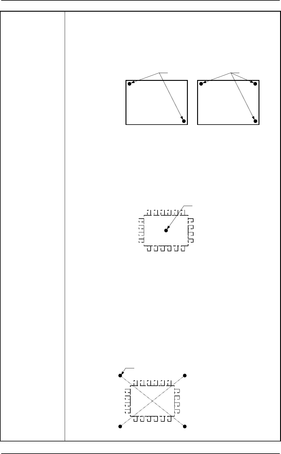
Example :
To correct the positional deviation covering the whole area of PCB (PCB
Overall Correction)
To improve recognition accuracy, put fiducial marks diagonally on two places of
PCB when the 2-point recognition mode is selected. In the case of 3-point
recognition mode, put two fiducial marks diagonally and one fiducial mark close to
one of the remaining corners.
PCB
Fiducial Mark
PCB
Fiducial Mark
Example 1 :
To correct the positional deviation of component placement points
(1-point recognition)
Put a fiducial mark on the center of component placement point or
a desired point around the center.
Recommended Position: Center of Component Placement Point
•
This position is effective when the positional deviation covering the whole
area of PCB is corrected.
When the PCB overall correction operation is performed, the theta (angle)
correction is also made. The fiducial mark described here is used to correct
the placement position.
Fiducial Mark
Example 2 :
To correct the component placement point
(2-point recognition)
Put fiducial marks on the desired two points around the center of
component placement point.
Recommended Position : Point Symmetry
It is recommended that two points (fiducial marks)
should be located symmetrically on both sides of the
center of the placement position.
(A-A'/B-B')
•
These fiducial marks are used to correct the component position and the
theta (angle).
The 2-point recognition is effectively to correct deviated and distorted part
of the printing patterns.
Fiducial Mark
A
A'B
B'
2. Specifications
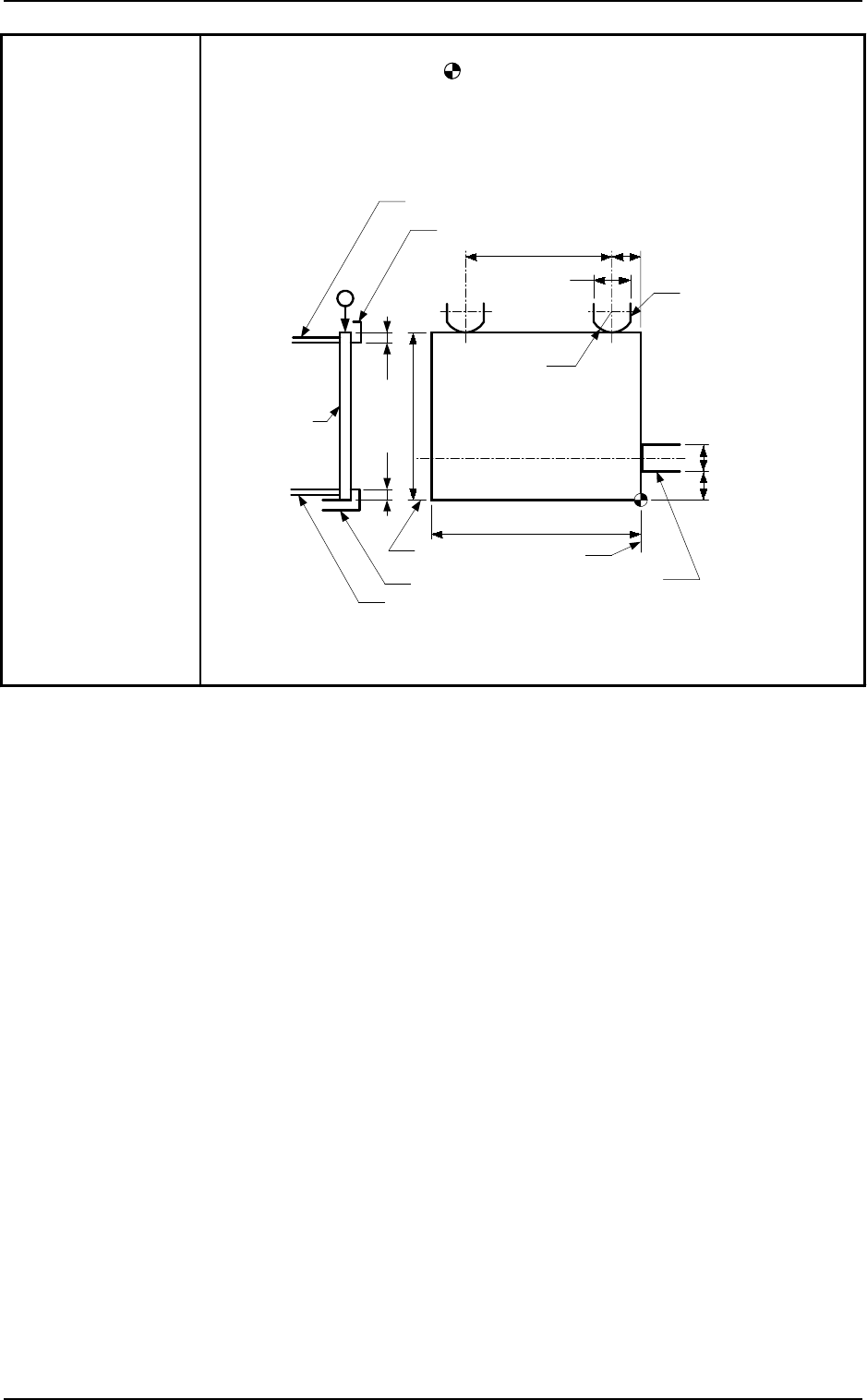
9910-001 1-5 Tg0246-PM-OP
PCB Clamping: Mechanical Clamping
Note : The center of the mark is the reference point.
The reference point and plane differ depending on the contents of
the specifications. There is no change in the distances between the
reference point and the PCB stopper and between the reference
plane and the Y pusher. Consult our sales personnel for details.
11
PCB
PCB Stopper
(either one of the right and left stoppers)
Clamp Plate on Fixed Side
Fixed Chute
Movable Chute
Clamp Plate on Movable Side
R20
27
58
×
7
10
6
50
t
o
381
50
t
o
460
Y Pusher
Reference
Plane
Reference
Plane
2.5 2.5
Unit : mm
2. Specifications
9910-001 1-6 Tg0246-PM-OP
5. Conditions of PCB
before Placement
Max. 30
3.5
PCB
φ
3
φ
2
PCB Support Pin
(The figure is based on the assumption that
the PCB is being transferred.)
Range (Shadowed Area) where
previously-placed components
should not be placed
Component
2.8
PCB Support Pin (Several Places)
Notes :
3.5
Max. 25.4
3.5 3.5
(a) The pin can be shifted at "40 mm" pitch.
(The shifting is partly possible at "10 mm" or "20 mm" pitch.)
(b) Set the Support pins such that they do not touch the already placed
components.
(c) The figure shows that the PCB is being supported.
Note :
The dimensions are those for design reference. Leave some room for
the actual setting.
6. Component
Placeable Range
Glue
SOP
Cream Solder
QFP
Min. 3.5
Min. 3.8
Min. 3.5
Reference Plane
Upper Surface of
P.C.B.
QFP
PCB
Max. 25.4
Reference Plane
11
PCB Stopper
(either one of the right and left stoppers)
6
19
19
PCB Stopper
(either one of the right and left stoppers)
Notes : (a) The above figure shows that the vacuum nozzles are not
protruding from the outer shapes of components.
Consult our sales personnel for details.
(b) Components cannot be placed in the shadowed area.
(c) Components cannot be placed in the range
(0.5 mm) around the opening such as a hole.
(d) The center of the mark is the reference point.
The reference point and plane differ depending on the contents
of the specifications. There is no change in the distance between
the reference point and the PCB stopper. Consult our sales
personnel for details.
7. Placement Time
Chip-Type Components : Approx. 0.46 sec/pc. (Highest Speed)
ICs (SOP/QFP) : Approx. 0.46 sec/pc. (Highest Speed)
BGA/CSP/FC : Approx. 0.9 sec/pc. (Highest Speed)
Notes : (a) PCB transition time is not included in the placement time under
optimum conditions.
(b) The placement time changes depending on feeder types and
requirements for component placement.
Consult our sales personnel for details.
Unit : mm
Unit : mm