Programming_mail.pdf - 第125页
III- 51 Programming Manual Part III Inspection Algorithm Step5: This is the parameter setting for lead length inspection. Select Lead length judgement from the Inspection parameter drop-down list. It calculates the avera…
III-50
Programming Manual
Part III Inspection Algorithm
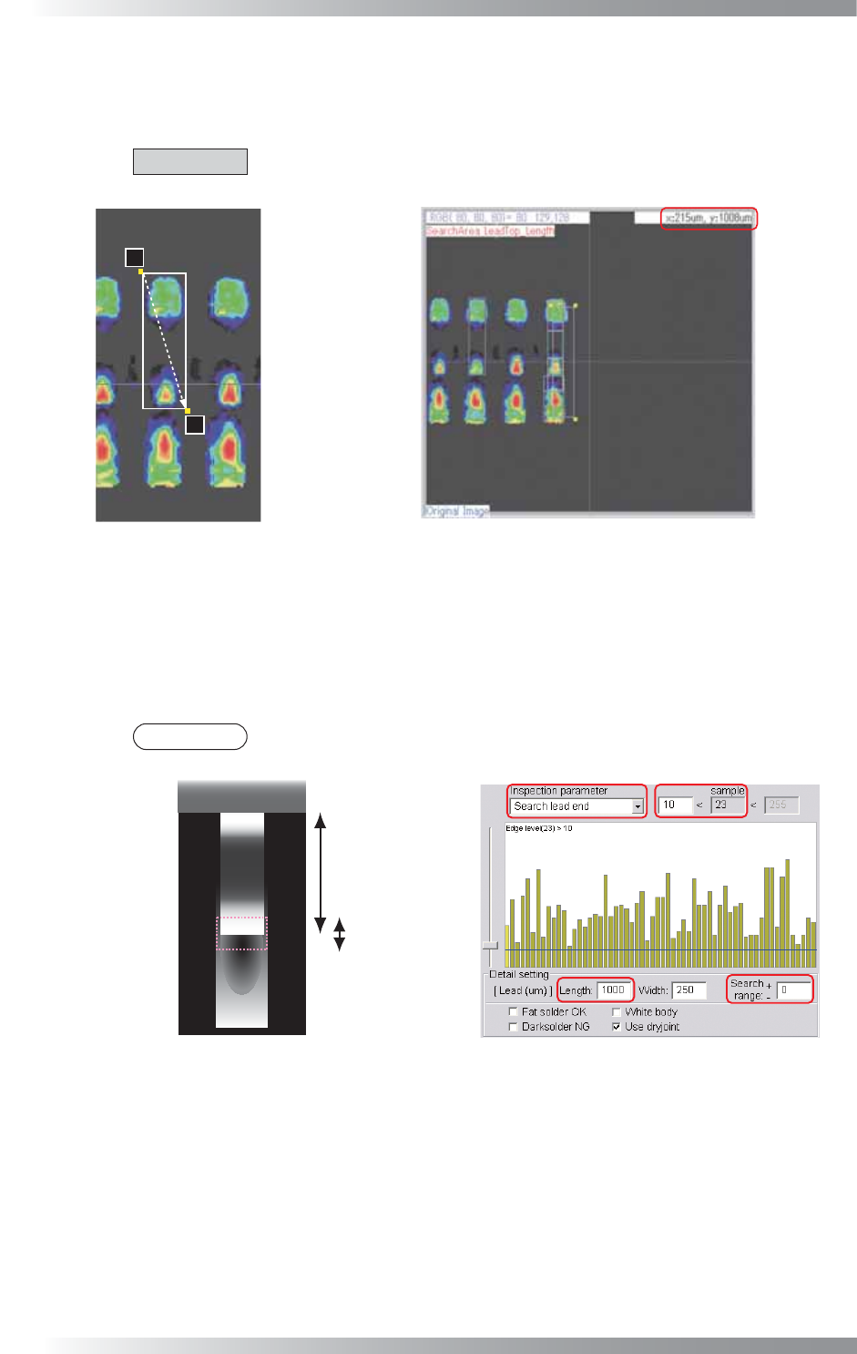
Step2: Length and Width will be displayed in the upper right corner of the dialog if left-clicking a
lead base and dragging the pointer to opposite corner of the lead end. Enter the window
size shown in the upper right side of the dialog in Length and Width.
CAUTION
Do not measure the lead size in the selected inspection window, otherwise the
inspection window is misaligned.
㪉
㪈
Lead Base
Gull Wing Area
Lead End
Pad Lead Area
Pad Center Area
Pad End Area
Body of IC Component
Measure by another pin
Figure 1-60 Enter
Length
and
Width
Step3: It automatically locates the edge of lead end area and pad lead area by searching the edge
of lead end and solder. Select Search lead end from the Inspection parameter drop-down
list. Make sure that the pink dotted area includes both edges of the lead end area and
solder. If the search range is too small or too large, change the Search range value to
adjust search area size.
NOTE
The center of the search area is at the lead end area. Adjust the search area size
by changing the Search range value.
Lead length
Search range
Lead Base Area
Lead End Area
Pad Lead Area
Figure 1-61 Adjust Search range
Step4: Enter the brightness level difference between the lead end and pad lead area in the left side
of Sample. In the search area, the algorithm calculates maximum brightness level minus
minimum brightness level as the sample value. If the sample value is larger than the OK
range, the lead end will be located. Default is 10. Adjust parameters according to the solder
condition.
III-51
Programming Manual
Part III Inspection Algorithm
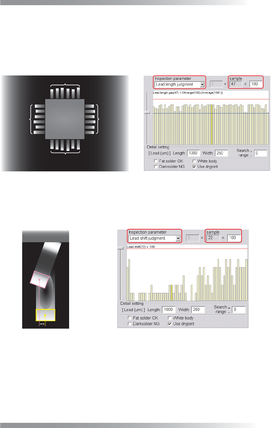
Step5: This is the parameter setting for lead length inspection. Select Lead length judgement from
the Inspection parameter drop-down list. It calculates the average value of leads length in
the same side of the component. The difference in amount between average length and
actual lead length is shown as the sample value. If the sample value is lower than OK range,
the result will be OK. The inspection logic is same as Part III 1.22 AS_Av_LeadLength.
Default is 100 [μm]. If necessary, change the value according to inspection accuracy.
Average value for leads length
Average
Average
Average
Average
in the same side of the body
- Selected lead length
Figure 1-62 Lead Length Judgement
Step6: This is the parameter setting for lead shift inspection. Select Lead shift judgement from the
Inspection parameter drop-down list. The shift amount from lead end area and pad end
area is shown as sample value. If the sample value is lower than OK range, the result will be
OK. Default is 100 [μm]. If necessary, change the value depends on inspection accuracy.
Lead End Area
Pad End Area
Figure 1-63 Lead Shift Judgement
III-52
Programming Manual
Part III Inspection Algorithm
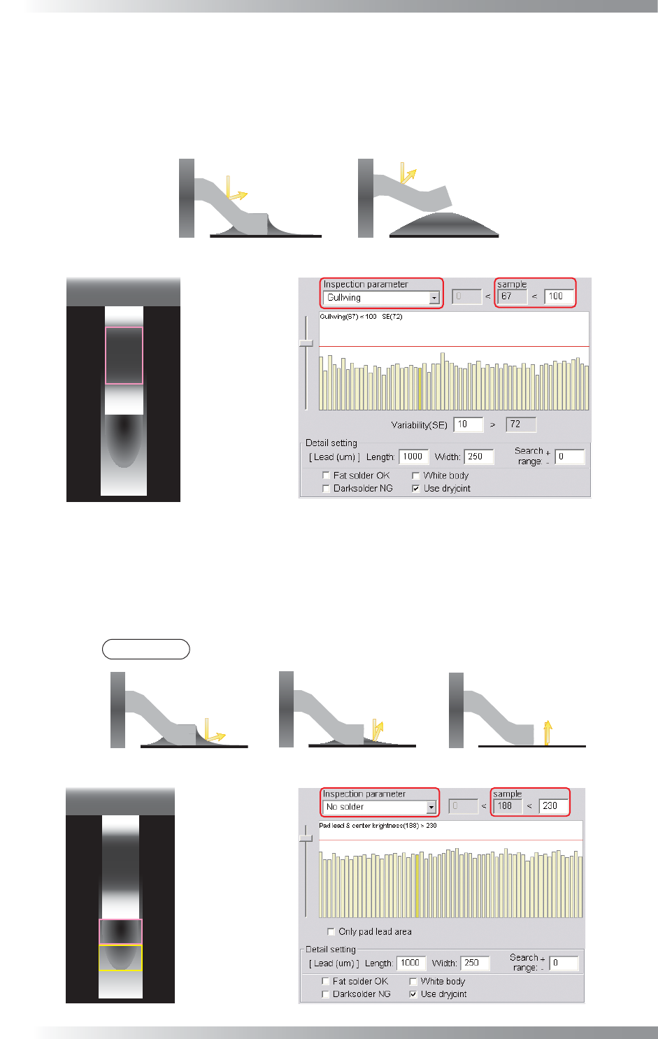
Step7: This is the parameter setting for lead bend inspection. Select Gullwing from the Inspection
parameter drop-down list. It calculates the average brightness value of gull wing area in the
same side of the component. The difference in amount between average brightness and actual
brightness is shown as the sample value. If the sample value is lower than OK range, the result
will be OK. Default is 100. If necessary, change the value according to inspection accuracy.
(a) Normal
(b) LiftedLead
High Brightness Low Brightness
Gull Wing Area
Figure 1-64 Lead Bend Inspection
Step8: This is the parameter setting for solder inspection. Select No solder from the Inspection
parameter drop-down list. It calculates average brightness level in pad lead area and pad
center area as sample value. If the sample value is lower than OK range, the result will be
OK. Default is 230. If necessary, change the value depends on inspection accuracy.
NOTE
The average brightness level is lower in case of no solder or insuffi cient solder.
(a) Normal
(b) Insufficient Solder
Low Brightness High Brightness
(c) No Solder
High Brightness
Pad Center Area
Pad Lead Area
Figure 1-65 Solder Inspection