Programming_mail.pdf - 第238页
V- 48 Programming Manual Part V Inspection Data 4.6 Clinch Pin Inspection Setting Clinch pin inspection detects width of the top of the clinch pin. This algorithm veri fi es if there are pins or not. 4.6.1 Parameter of Cl…
V-47
Programming Manual
Part V Inspection Data
4.5.2 Setting Procedure of Straight Pin Inspection
Step1: Press PIN button.
Step2: Check Inspect Pin.
Step3: Press the straight pin icon (
).
Step4: Check Dedicated.
Step5: Enter values in Y width and X width fi eld to set the size of the straight pin. Press Inspect.
Make sure that the straight pin is surrounded by the pink window.
NOTE
If the straight pin is not detected by Dedicated, check Top
NOTE
The inspection area is the area where surrounded by the pink window.
Step6: Enter a value in Lower limit fi eld.
NOTE
Detected will be high if an inspection area is bright and its surroundings are dark.
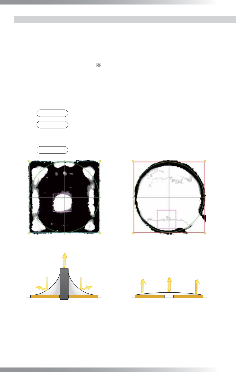
(a)Normal(Detected value is 59 ) (b)No Pin(Detected value is 2 )
Straight Pin
(Bright)
Solder
(Dark)
Solder
(Dark)
Solder
(Bright)
Solder
(Bright)
Solder
(Bright)
Figure 4-10 Straight Pin Inspection
V-48
Programming Manual
Part V Inspection Data
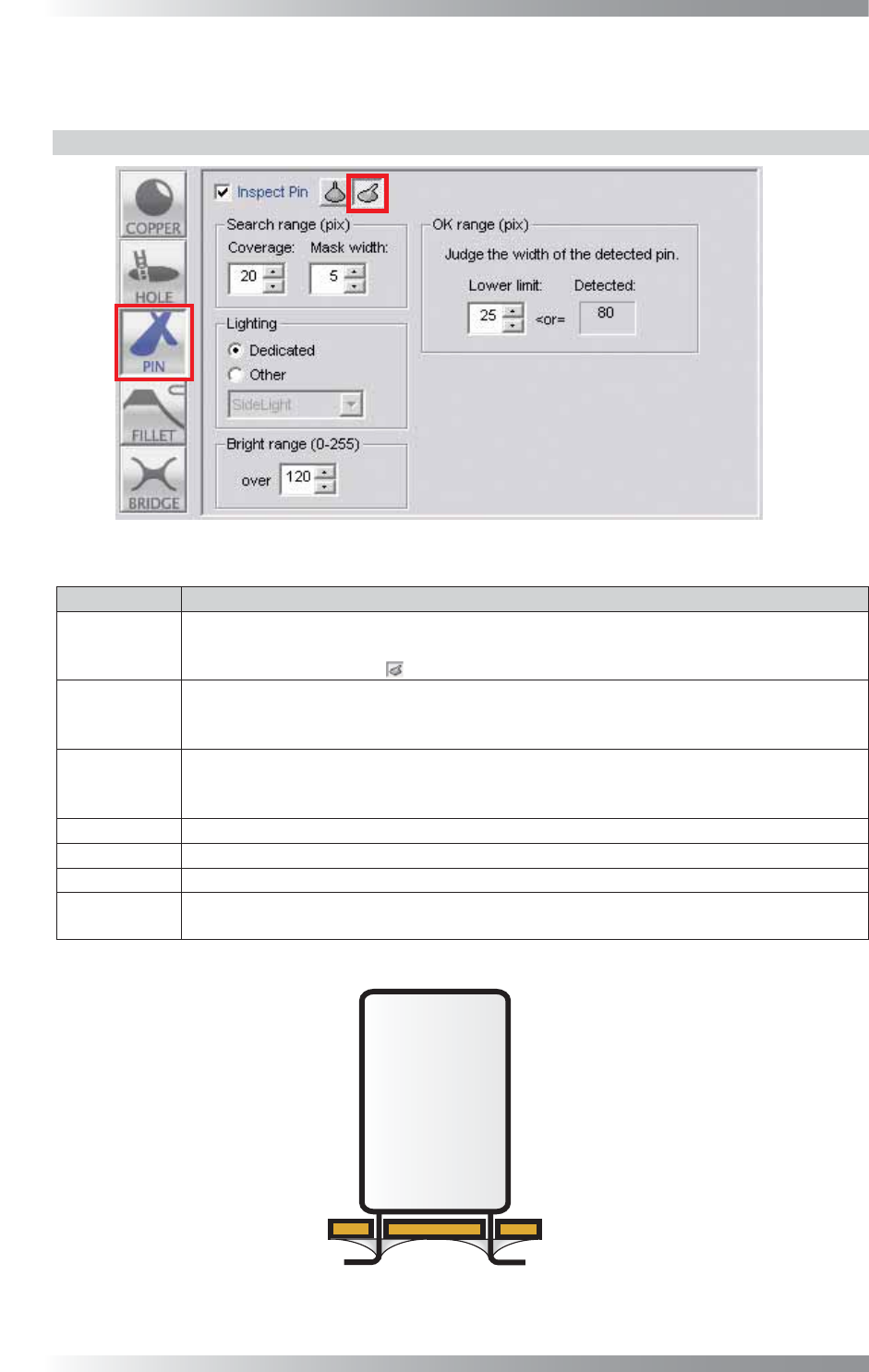
4.6 Clinch Pin Inspection Setting
Clinch pin inspection detects width of the top of the clinch pin. This algorithm verifi es if there are pins or not.
4.6.1 Parameter of Clinch Pin Inspection
Figure 4-11 Clinch Pin Inspection Setting
Parameter Description
Inspect Pin
To activate pin inspection, check Inspect Pin.
To disable Pin inspection, un-check Inspect Pin. Buttonʼs color is displayed as gray.
Press the clinch pin icon (
) to inspect clinch pins.
Coverage
The inspection area is specifi ed by width (pixel value) from the dotted line circle.
The inspection area is in the green circle except the area netted.
Enter the bigger value to enlarge the inspection area.
Mask width
Specifi es a “no inspection” area in an inspection area set in Coverage by a width (pixels)
from a dotted line circle.
Use this parameter if a pad edge is uneven. Set a mask so a solder fi llet is covered.
Lighting
Select a lighting. Default setting is Dedicated.
Bright range Shows the pixels of a specifi c brightness level which is set in Bright range in yellow.
Lower limit
Set the lower limit of an acceptable range.
Detected
Clinch pin inspection detects a border between a clinch pin end and a netted (masked)
area. The Detected value shows a width (pixels) of clinch pin end at the border.
Table 4-6 Parameter of Clinch Pin Inspection
Figure 4-12 Clinch Pin Inspection
V-49
Programming Manual
Part V Inspection Data
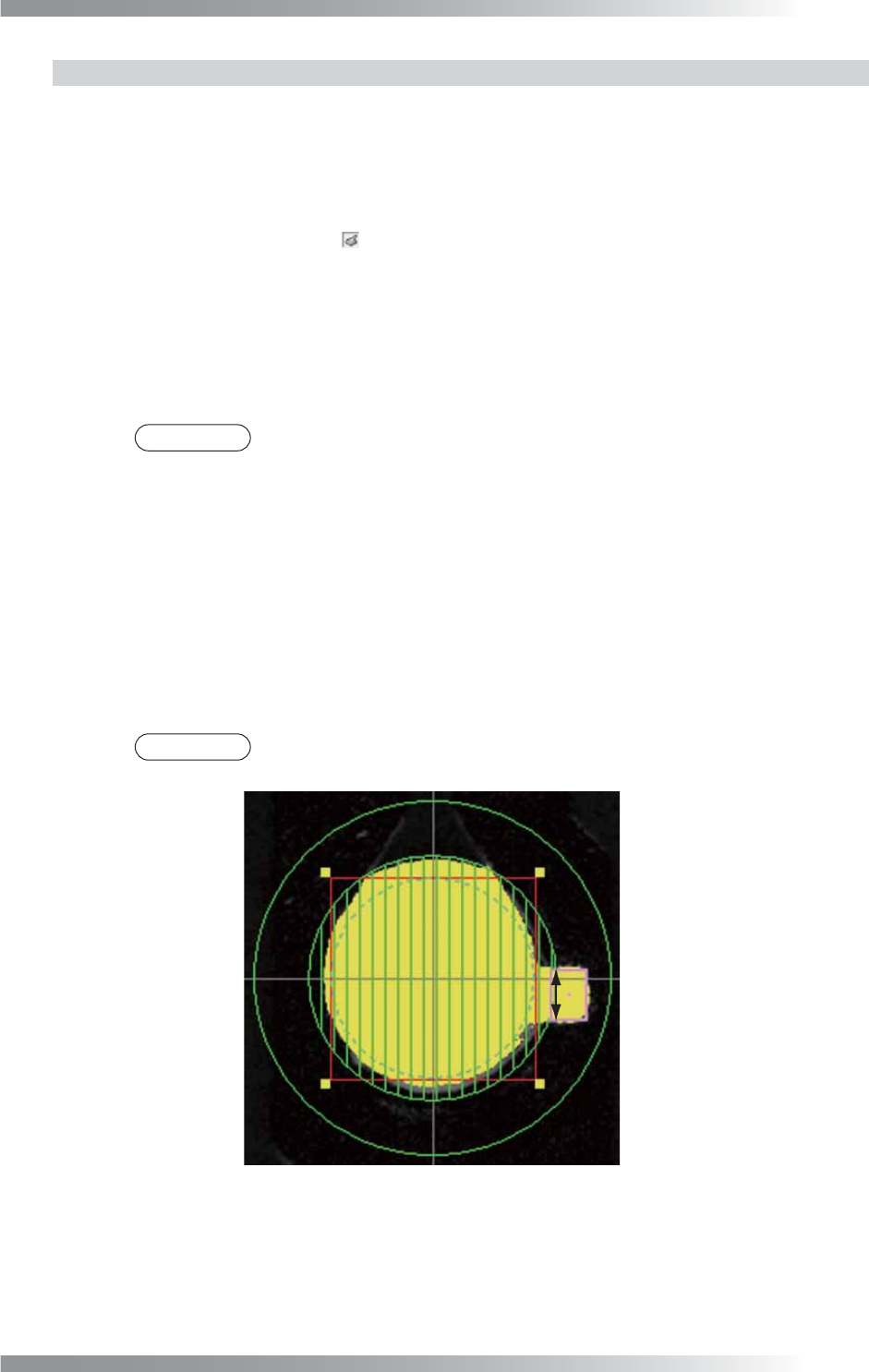
4.6.2 Setting Procedure of Clinch Pin Inspection
Step1: Press PIN button.
Step2: Check Inspect Pin.
Step3: Press the clinch pin icon (
).
Step4: Check Dedicated.
Step5: Adjust Coverage to surround the top of the clinch pin. The inspection area is specifi ed by
width (pixel value) from the dotted line circle. The inspection area is in the green circle
except the area netted. Enter the bigger value to enlarge the inspection area.
NOTE
If the solder and the top of the clinch pin are not visually clear by Dedicated, check
Other and select a lighting from the drop-down list.
Step6: Enter a value into the Mask width fi eld.
If the pad edge is uneven, specifi es a “no inspection” area in the inspection area set in
Coverage by the width (pixels) from the dotted line circle. Set the mask so the solder fi llet
is covered.
Step7: Enter the value in Bright range fi eld to detect the solder and the top of the clinch pin.
Step8: Enter a value into the Lower limit fi eld.
NOTE
Clinch pin inspection detects a border between a clinch pin end and a netted (masked)
area. The Detected value shows a width (pixels) of clinch pin end at the border.
Detected
Figure 4-13 Clinch Pin Inspection