Programming_mail.pdf - 第87页
III- 13 Programming Manual Part III Inspection Algorithm 1.5.3 Setting Procedur e Step1: Select SideLignt from the Lighting drop-down list. Step2: Enter the appropriate vector into the Shift fi eld by selecting from V1 to…
III-12
Programming Manual
Part III Inspection Algorithm
1.5 ChipMissing3
1.5.1 Inspection Overview
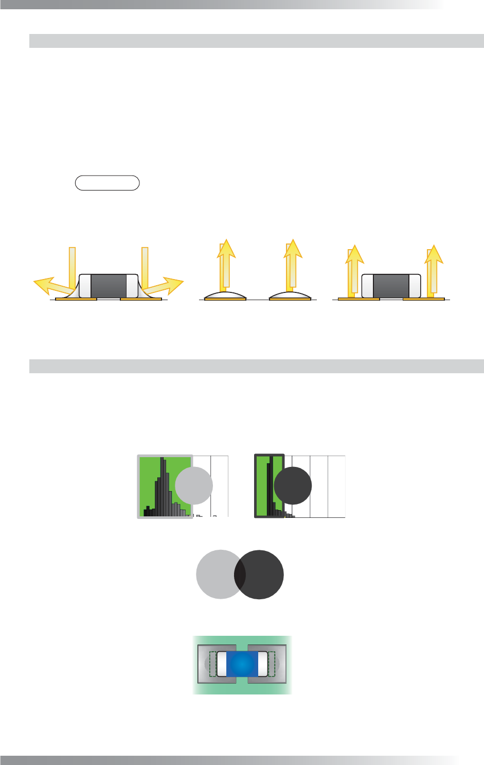
ChipMissing3 is the algorithm to inspect solder at either end of the chip component with TopLight and
SideLight used.
The brightness level of a solder is lower if a solder fi llet is formed. The brightness level of a solder is
higher if a solder fi llet is not formed, or a component is missing (refer to Figure 1-13).
ChipMissing3 is suitable for a chip missing inspection or solder inspection.
1.5.2 Parameter Setting
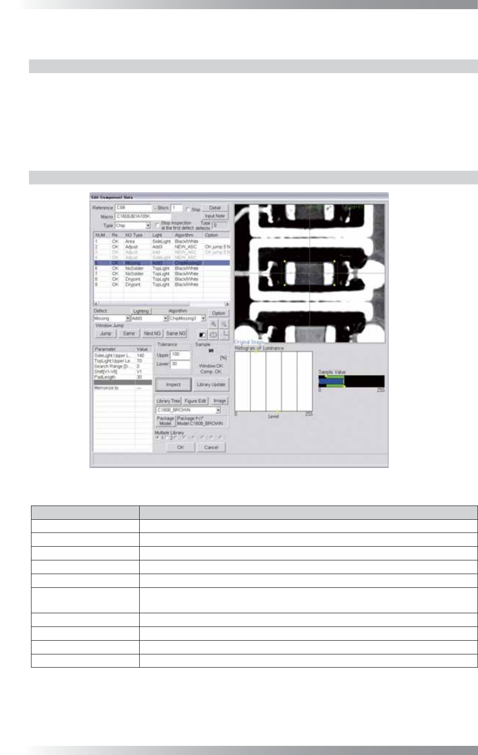
Figure 1-12 ChipMissing3
Parameter Description
Lighting Select SideLight.
Algorithm Select ChipMissing3.
SideLight Upper Level Upper limit of brightness level in OK range (SideLight).
TopLight Upper Level Upper limit of brightness level in OK range (TopLight).
Search Range[0-30] Enter 0.
Shift[V1-V8]
Enter the appropriate vector. Any value from V1 to V8 is available.
Select the vector according to the Memorize to fi eld of the Adjust window.
PAD Length Default is 30. Enter the bigger value to enlarge the inspection area.
Memorize to -
Upper, Lower Set the upper and lower limit of the OK range.
Sample Refer to Part III 1.5.4 Calculation of Sample Value.
Table 1-5 Parameter of ChipMissing3
III-13
Programming Manual
Part III Inspection Algorithm
1.5.3 Setting Procedure
Step1: Select SideLignt from the Lighting drop-down list.
Step2: Enter the appropriate vector into the Shift fi eld by selecting from V1 to V8 according to the
vector used in the Memorize to fi eld in the Adjust window.
Step3: Check if the sample value is in OK range. If it is out of OK range, change values in SideLight
Upper Level or TopLight Upper Level.
NOTE
If the inspection area is too small, change values in PAD Length to larger.
Step4: Press Inspect. Make sure that the inspection is completed properly.
(a) Normal (b) Missing (c) No Solder
Low Brightness High Brightness High Brightness
Figure 1-13 Missing / Solder inspection by ChipMissing3
1.5.4 Calculation of Sample Value
Set the OK brightness range of SideLight and TopLight by adjusting SideLight Upper Level /
TopLight Upper Level values. The percentages of the area that the result is OK in solder inspection
window at either end of the chip component with TopLight and SideLight are calculated.
The lower value is shown as the sample value.
㪇 㪏㪇 㪉㪌㪌㪈㪌㪇㪇 㪉㪌㪌
㪧㪘㪛㩷㪪㫀㪻㪼㩷㪤㪸㫏 㪧㪘㪛㩷㪫㫆㫇㩷㪤㪸㫏
㪐㪇㩼 㪏㪇㩼
Calculate the Rate of the Overlapping Parts
TopLightSideLight
TopLight
0䌾80
SideLight
0䌾150
Sample Value
OK Range
OK
Range
Figure 1-14 Calculation of Sample Value
III-14
Programming Manual
Part III Inspection Algorithm
1.6 Length
1.6.1 Inspection Overview
Length is the algorithm to inspect component’s length.
Surround the component and around it by a window. Component’s length is calculated based on the
changes of brightness level in the window.
If the inspected component’s length is in OK range, the result will be OK.
Length is suitable for missing inspection of chip components.
1.6.2 Parameter Setting
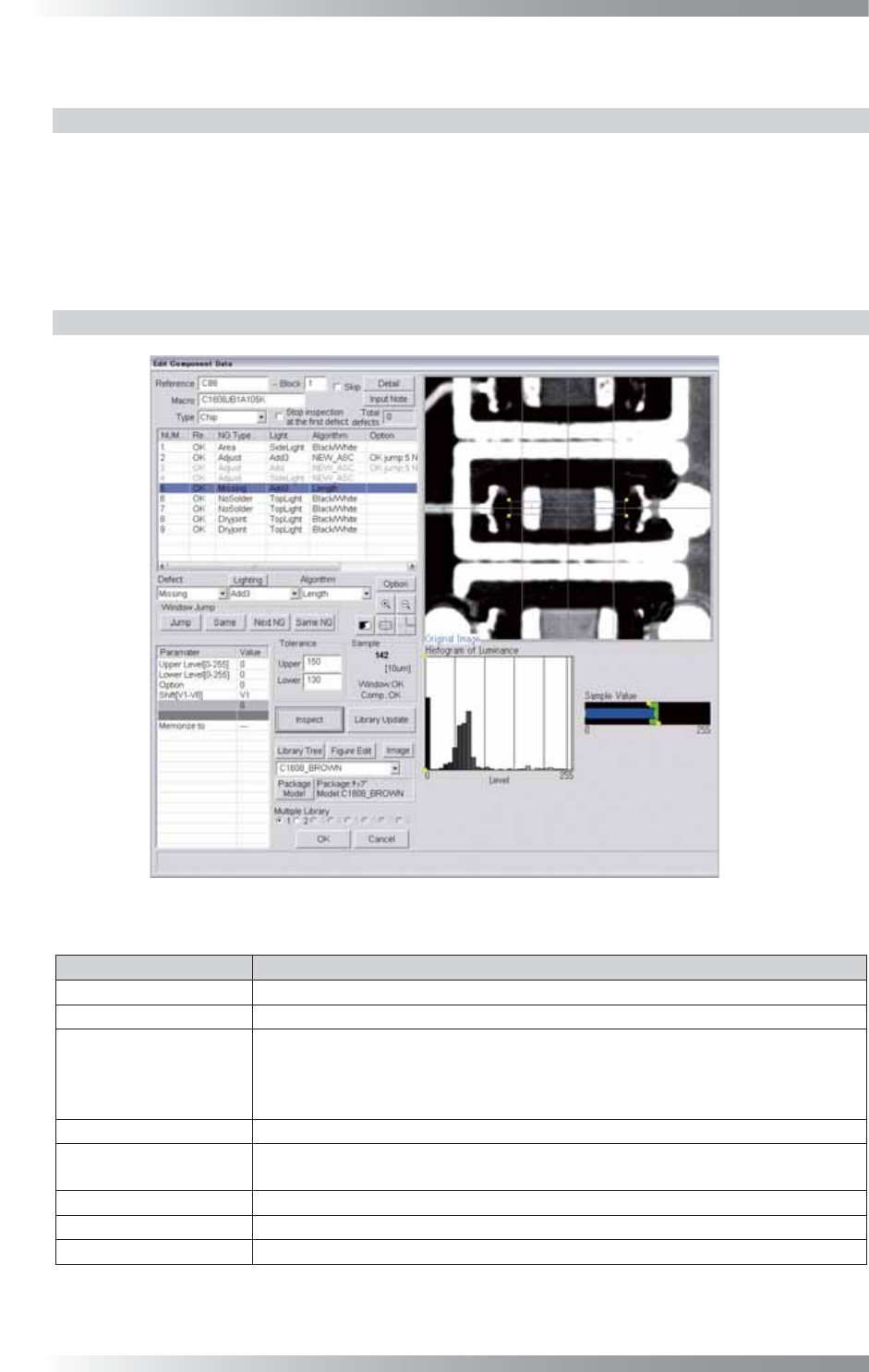
Figure 1-15 Length
Parameter Description
Lighting Select a lighting that the component is visually clear.
Algorithm Select Length.
Upper Level[0-255],
Lower Level[0-255]
Enter 0 in Upper Level and Lower Level if the component brightness level is
lower than the brightness level of a PCB.
Enter 255 in Upper Level and Lower Level if the component brightness level is
higher than the brightness level of a PCB.
Option Enter 0.
Shift[V1-V8]
Enter the appropriate vector. Any value from V1 to V8 is available.
Select the vector according to the Memorize to fi eld of the Adjust window.
Memorize to -
Memorize to Set the upper and lower limit of the OK range.
Sample
Shows the length of the component by 10 μm.
Table 1-6 Parameter of Length